
Method for growing quantum well stress release layer of epitaxial structure and epitaxial structure

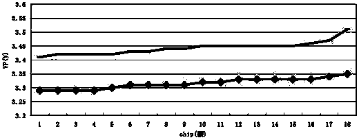
A stress release, epitaxial structure technology, applied in electrical components, circuits, semiconductor devices, etc., to achieve the effect of increasing the directional voltage, improving the recombination efficiency, and reducing the working voltage VF

Active Publication Date: 2013-11-27
XIANGNENG HUALEI OPTOELECTRONICS
View PDF6 Cites 12 Cited by
  • Summary
  • Abstract
  • Description
  • Claims
  • Application Information

AI Technical Summary

Problems solved by technology

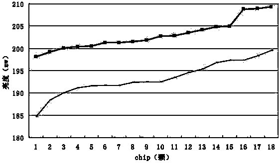
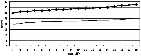
[0004] The purpose of the present invention is to provide a growth method of an epitaxial structure quantum well stress release layer and its epitaxial structure to solve the technical problem of further improving LED brightness

Method used


Image

  • Method for growing quantum well stress release layer of epitaxial structure and epitaxial structure
  • Method for growing quantum well stress release layer of epitaxial structure and epitaxial structure
  • Method for growing quantum well stress release layer of epitaxial structure and epitaxial structure

Examples


Embodiment 1

[0062] The invention uses Aixtron Cruis I MOCVD to grow high-brightness GaN-based LED epitaxial wafers. Using high-purity H 2 or high purity N 2 or high purity H 2 and high purity N 2 The mixed gas as the carrier gas, high-purity NH 3 As N source, metal-organic source trimethylgallium (TMGa), triethylgallium as gallium (TEGa) source, trimethylindium (TMIn) as indium source, N-type dopant as silane (SiH 4 ), the P-type dopant is magnesium dicene (CP 2 Mg), the substrate is (0001) sapphire, and the reaction pressure is between 100mbar and 800mbar. The specific growth method is as follows:

[0063] 1. In the reaction chamber of 800-1000℃, 300mbar, 33000sccm hydrogen gas is introduced, and the sapphire substrate is treated at high temperature for 5-6 minutes;

[0064] 2. Lower the temperature to 500-550°C, and grow a low-temperature buffer layer GaN (Nucleation) with a thickness of 30-40nm on the sapphire substrate;

[0065] 3. Raise the temperature to 1000-1100°C, and con...


PUM

PropertyMeasurementUnit
Thicknessaaaaaaaaaa
Thicknessaaaaaaaaaa
Thicknessaaaaaaaaaa

Abstract

The invention provides a method for growing a quantum well stress release layer of an epitaxial structure and the epitaxial structure. The epitaxial structure comprises the quantum well stress release layer with the total thickness of 160nm. The quantum well stress release layer is an HT MQW layer doped with In and Al and comprises a GaN layer with the thickness of 40nm and an AlyInxGa(1-x-y)N layer with the thickness of 2nm, wherein x ranges from 0.05 to 0.08, and y ranges from 0.02 to 0.05. According to the growing method, by modifying the energy band diagram of the HT MQW, electrons entering a luminous zone can be blocked, and the probability that the electrons enter a p layer and are recombined with holes in a nonradiative mode is reduced; moreover, the electrons blocked in the HT MQW are injected into the luminous zone more evenly through two-dimensional diffusion, the efficiency of the recombination between the electrons and the holes is promoted, and the luminance is improved.

Description

technical field [0001] The invention relates to the technical field of LED epitaxial design, in particular to a growth method of a quantum well stress release layer with an epitaxial structure and an epitaxial structure thereof. Background technique [0002] GaN-based light-emitting diode (LED), as a new type of high-efficiency, environmentally friendly, and green solid-state lighting source, has the advantages of low voltage, low power consumption, small size, light weight, long life, and high reliability, and is rapidly being widely used. Widely used in traffic signal lights, mobile phone backlights, outdoor full-color display screens, urban landscape lighting, automotive interior and exterior lights, tunnel lights, etc. [0003] Therefore, the performance improvement of LEDs in all aspects has been focused on by the industry. Contents of the invention [0004] The purpose of the present invention is to provide a growth method of an epitaxial structure quantum well stre...

Claims


Application Information

Patent Timeline
IPC IPC(8): H01L33/12
Inventor 农明涛
Owner XIANGNENG HUALEI OPTOELECTRONICS
Learn More