
Shallow quantum well growth method for increasing light emitting efficiency of GaN-based LED (Light-Emitting Diode)

A shallow quantum well and growth method technology, applied in the field of GaN material preparation, can solve problems such as limited effects, achieve good interception and storage effects, improve recombination efficiency, and reduce V-type defects

Inactive Publication Date: 2013-01-30
合肥彩虹蓝光科技有限公司
View PDF5 Cites 16 Cited by
  • Summary
  • Abstract
  • Description
  • Claims
  • Application Information

AI Technical Summary

Problems solved by technology

The above method improves the radiative recombination efficiency of quantum wells to a certain extent, but the effect is limited

Method used


Image

  • Shallow quantum well growth method for increasing light emitting efficiency of GaN-based LED (Light-Emitting Diode)
  • Shallow quantum well growth method for increasing light emitting efficiency of GaN-based LED (Light-Emitting Diode)

Examples


Embodiment Construction

[0017] The embodiments of the present invention are described in detail below: the present embodiment is implemented on the premise of the technical solution of the present invention, and provides a detailed implementation manner and a specific operation process, but the protection scope of the present invention is not limited to the following implementations example.

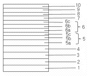
[0018] like figure 1 As shown, the LED epitaxial structure provided by the present invention includes: a substrate layer 1, a low-temperature GaN buffer layer 2, an undoped high-temperature GaN buffer layer 3, a Si-doped n-type GaN layer 4, a shallow quantum well 5, and a plurality of light-emitting layers. A quantum well 6 , a low temperature p-type GaN layer 7 , a p-type AlGaN electron blocking layer 8 , a high-temperature p-type GaN layer 9 , and a p-type GaN contact layer 10 .

[0019] The specific implementation steps of the method for improving the GaN-based LED shallow quantum well growth structure and ...


PUM


Abstract

The invention relates to a shallow quantum well growth method for increasing the light emitting efficiency of a GaN-based LED (Light-Emitting Diode). The epitaxial wafer structure of the LED sequentially comprises a substrate layer, a low-temperature GaN buffer layer, an undoped high-temperature GaN buffer layer, a Si doped n type GaN layer, a luminous-layer multiple-quantum well, a low-temperature p type GaN layer, a p type AlGaN electron blocking layer, a high-temperature p type GaN layer and a p type GaN contact layer from bottom to top. The luminous-layer multiple-quantum well sequentially comprises a low-temperature shallow quantum well and a low-temperature multiple-quantum well luminous layer structure from bottom to top, wherein the low-temperature shallow quantum well is composed of three parts of shallow quantum wells. According to the method, a quantum-well-structure gallium nitride base material with high crystallization quality and high luminous efficiency can be effectively obtained, and a gallium nitride system LED with high luminescent intensity is obtained.

Description

[0001] technical field [0002] The invention belongs to the technical field of GaN-based material preparation, and more particularly relates to a method for improving luminous efficiency by improving the growth structure of shallow quantum wells in GaN-based LED quantum wells. [0003] Background technique [0004] GaN-based materials are ionic crystals. Since the positive and negative charges do not overlap, spontaneous polarization is formed; in addition, due to the lattice adaptation between InGaN and GaN materials, piezoelectric polarization will be induced, thereby forming a piezoelectric polarization field. The existence of the polarization field reduces the equivalent band gap of the quantum well and red-shifts the emission wavelength; on the other hand, the overlap of the electron and hole wave functions will decrease, reducing the probability of their radiative recombination. Another reason that affects the luminous efficiency of the quantum well: the electrons...

Claims


Application Information

Patent Timeline
Patent Type & Authority Applications(China)
IPC IPC(8): H01L33/06H01L33/00
Inventor 李永王耀国钟尹泰
Owner 合肥彩虹蓝光科技有限公司
Learn More