Power semiconductor module assembled through three-dimensional structural units

A power semiconductor, three-dimensional structure technology, applied in the direction of semiconductor devices, semiconductor/solid-state device components, electrical components, etc., can solve the problems of reducing the service life of modules, stripping of bonding wires, uneven cooling channel structure, etc., to enhance heat dissipation capacity, increased power density, and improved thermal performance

Inactive Publication Date: 2013-11-27
INST OF ELECTRICAL ENG CHINESE ACAD OF SCI
View PDF10 Cites 4 Cited by
  • Summary
  • Abstract
  • Description
  • Claims
  • Application Information

AI Technical Summary

Problems solved by technology

The junction temperature of the power semiconductor module chip may reach 175°C or even higher during operation. Excessively high chip junction temperature will greatly reduce the number of cycles of the power semiconductor module and reduce the service life of the module.
[0003] In current power semiconductor modules, metal bonding wires are used for the connection between IGBTs and diodes. This method easily causes the bonding wires to peel off due to thermal fatigue under high temperature conditions, which greatly reduces the reliability of the module.
In this traditional packaging structure, bonding wires are used on the front side of the chip for electrical interconnection. Therefore, the chip as a heat source can only dissipate heat by soldering DBC and copper base plate structure on the back side, while the heat dissipation efficiency of the traditional single-sided heat dissipation structure is very limited.
[0004] In addition, due to the uneven cooling channel structure of high heat flux power devices, the uneven temperature distribution on the surface of the heat source chip is more prominent
The current modules are generally packaged by direct soldering to the copper base plate, which makes the failure of a certain unit lead to the scrapping of the entire module, and the other intact unit parts cannot be further used, which increases the cost of use
[0005] The power semiconductor modules proposed in US patents US0138452A1 and US7005743B2 adopt the method of double-sided cooling, which improves the cooling effect of the module, but the gate of the power semiconductor chip described in this patent is drawn out by bonding wires, and the entire packaging process is still not Get rid of the dependence on bonding wires, which increases the process complexity of packaging

Method used


Image

  • Power semiconductor module assembled through three-dimensional structural units
  • Power semiconductor module assembled through three-dimensional structural units
  • Power semiconductor module assembled through three-dimensional structural units

Examples


Embodiment Construction

[0026] The present invention will be further described below in conjunction with the accompanying drawings and specific embodiments.

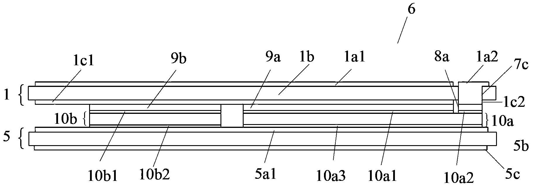
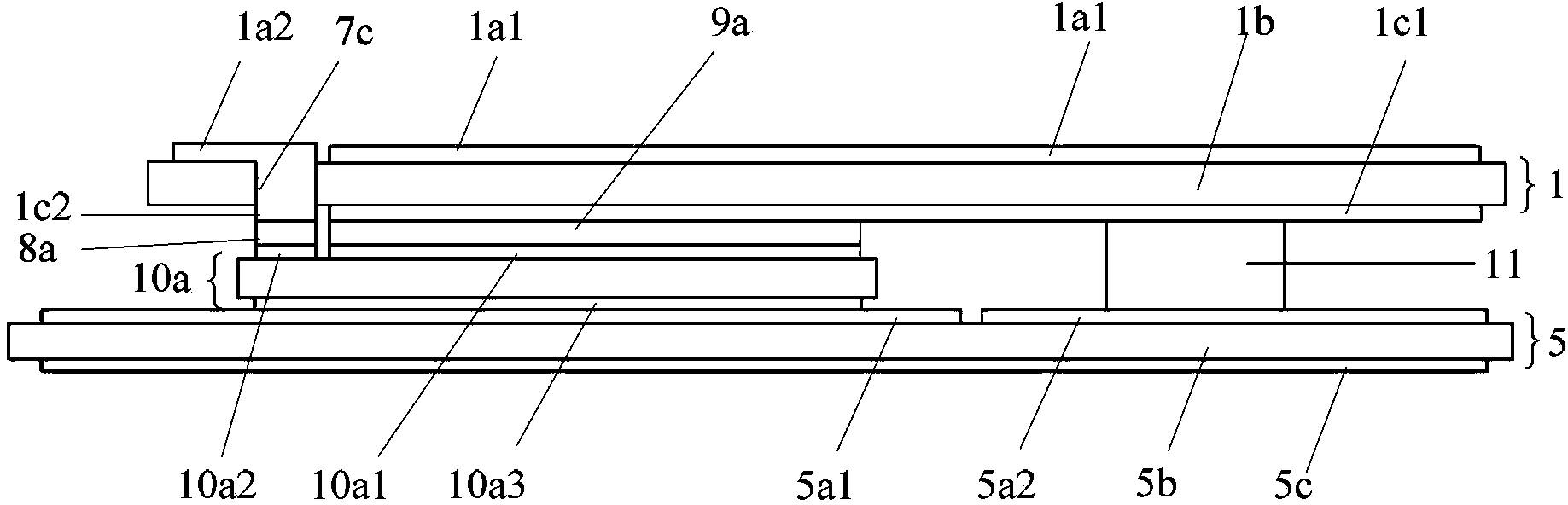
[0027] The power semiconductor module of the present invention is composed of multiple three-dimensional structural units, and each three-dimensional structural unit is fixedly installed on the insulating base plate. The emitter of one three-dimensional structure unit is connected in series with the collector of another three-dimensional structure unit through the connection terminal to form a half-bridge unit, and multiple half-bridge units are connected in parallel.

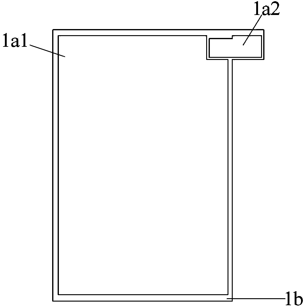
[0028] Such as Figure 1a As shown, the three-dimensional structure unit 6 includes a fully controlled power semiconductor chip 10a, an uncontrolled power semiconductor chip 10b, a first substrate 1, a second substrate 5, a first metal pad 8a, and a second metal pad 9a, And the third metal gasket 9b. The fully controlled power semiconductor chip 10a and the uncontrolled power s...


PUM


Abstract

The invention provides a power semiconductor module assembled through three-dimensional structural units. The power semiconductor module is assembled mechanically through the multiple three-dimensional structural units (6). An emitting electrode of one three-dimensional structural unit is connected with a collector electrode of another three-dimensional structural unit in series through a connector to form a half-bridge unit, and the multiple half-bridge units are in parallel connection. Each three-dimensional structural unit (6) of the power semiconductor module is composed of an all-control type power semiconductor chip (10a), a non-control type power semiconductor chip (10b), a first substrate (1) and a second substrate (5), wherein the all-control type power semiconductor chip (10a) and the non-control type power semiconductor chip (10b) are located between the first substrate (1) and the second substrate (5) and arranged side by side, and a grid electrode (10a2) of the all-control type power semiconductor chip (10a) is located at one corner of the non-control type power semiconductor chip (10b). The power semiconductor module is filled with insulation cooling liquid to be cooled.

Description

technical field [0001] The invention relates to a three-dimensional packaged power semiconductor module. Background technique [0002] In recent years, with the development of new energy technology, high-power converters have been widely used. The heat dissipation capability of the inverter becomes a core issue of common concern. The junction temperature of the chip of the power semiconductor module may reach 175°C or even higher during operation. Excessively high chip junction temperature will greatly reduce the number of cycles of the power semiconductor module and further reduce the service life of the module. [0003] In current power semiconductor modules, metal bonding wires are used for the connection between IGBTs and diodes. This method is likely to cause peeling of bonding wires due to thermal fatigue under high temperature conditions, which greatly reduces the reliability of the module. In this traditional packaging structure, bonding wires are used on the front...

Claims


Application Information

Patent Timeline
Patent Type & Authority Applications(China)
IPC IPC(8): H01L23/488H01L23/473
CPCH01L24/33H01L2924/13055H01L2924/00
Inventor 王春雷郑利兵方化潮靳鹏云韩立
Owner INST OF ELECTRICAL ENG CHINESE ACAD OF SCI
Why Eureka
Try Eureka