Etching-based one-dimensional electron gas gan-based hemt device and fabrication method
An electronic gas and device technology, applied in the field of microelectronics, can solve the problems of limited electron concentration, small breakdown electric field, poor electron transport characteristics, etc., to achieve good power characteristics, improve high temperature and high pressure characteristics, and improve power characteristics.
- Summary
- Abstract
- Description
- Claims
- Application Information
AI Technical Summary
Problems solved by technology
Method used
Image
Examples
Embodiment 1
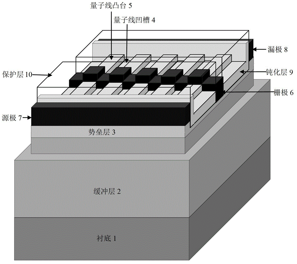
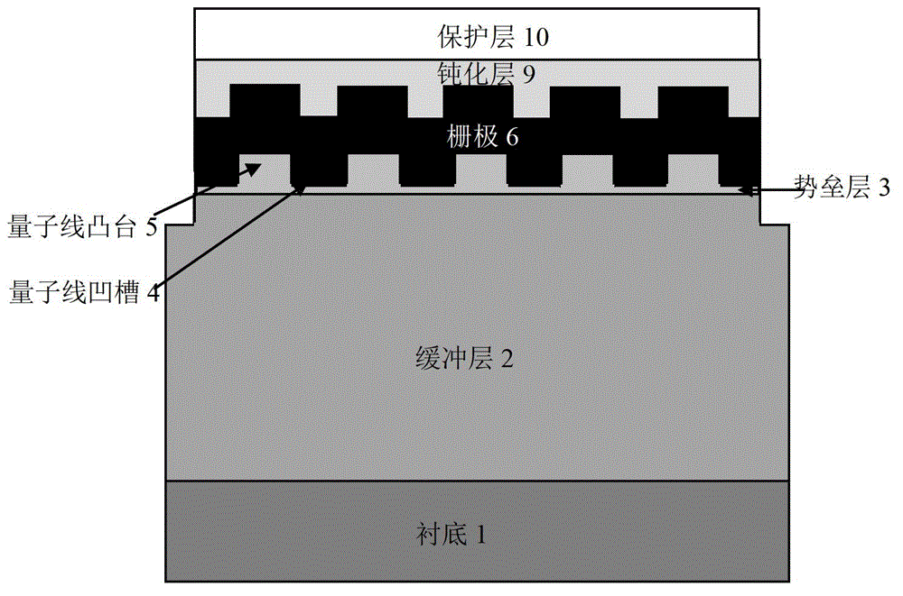
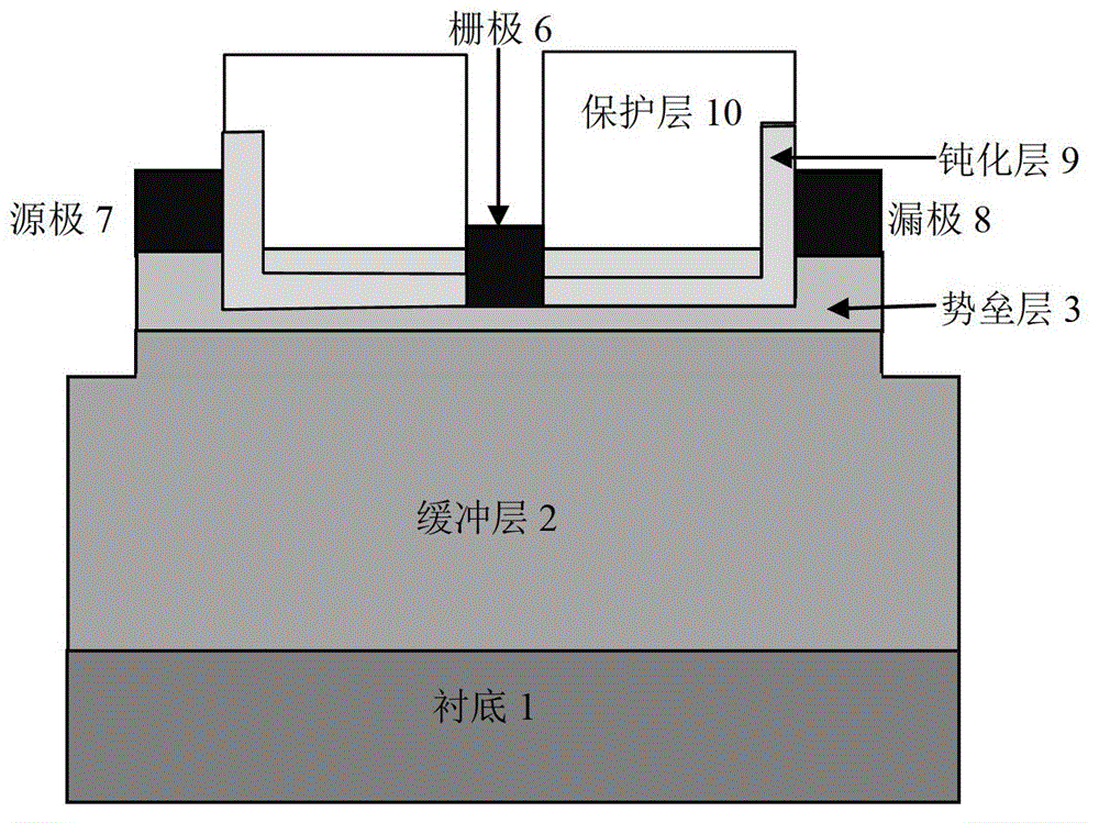
[0051] Embodiment 1, the production substrate 1 is sapphire, the buffer layer 2 is GaN, the barrier layer 3 is AlGaN, the passivation layer 9 is SiN, the protective layer 10 is SiN, the depth of the quantum wire groove 4 is 8nm, and the width is 50nm. A one-dimensional electron gas GaN-based HEMT with a width of 10 nm of quantum wire bosses 5 and a periodic arrangement of quantum wire grooves 4 and quantum wire bosses 5 .
[0052] Step 1, using MOCVD to epitaxially GaN semiconductor material with a thickness of 1 μm on the sapphire substrate 1 as the buffer layer 2; the process conditions for the epitaxial GaN buffer layer 2 are: the temperature is 1000°C, and the pressure is 200 Torr , the hydrogen flow rate is 4800 sccm, the ammonia gas flow rate is 4800 sccm, and the gallium source flow rate is 200 μmol / min.
[0053] Step 2: Deposit an AlGaN semiconductor material with a thickness of 10 nm on the buffer layer 2 by MOCVD as a barrier layer 3, and the Al composition of the Al...
Embodiment 2
[0070] Embodiment 2, the production substrate 1 is silicon carbide, the buffer layer 2 is GaN, the barrier layer 3 is AlGaN, the passivation layer 9 is SiN, and the protective layer 10 is SiO 2 , the quantum wire groove 4 has a depth of 28nm, a width of 250nm, a quantum wire boss 5 width of 50nm, and a one-dimensional electron gas GaN-based HEMT in which the quantum wire groove 4 and the quantum wire boss 5 are arranged periodically.
[0071] Step 1, epitaxially epitaxially GaN buffer layer 2 with a thickness of 3 μm on silicon carbide substrate 1 .
[0072] Using metal organic chemical vapor deposition MOCVD equipment under the process conditions of temperature 1020 ° C, pressure 200 Torr, hydrogen flow rate 5000 sccm, ammonia gas flow rate 5000 sccm, gallium source flow rate 220 μmol / min, epitaxy on silicon carbide substrate 1 GaN buffer layer 2 with a thickness of 3 μm.
[0073] Step 2, depositing an AlGaN barrier layer 3 with a thickness of 30 nm on the GaN buffer layer 2...
Embodiment 3
[0097] Embodiment 3, the production substrate 1 is silicon, the buffer layer 2 is GaN, the barrier layer 3 is AlGaN, and the passivation layer 9 is SiO 2 , the protective layer 10 is SiN, the depth of the quantum wire groove 4 is 48nm, the width is 500nm, the width of the quantum wire boss 5 is 100nm, and the one-dimensional electron gas GaN of the quantum wire groove 4 and the quantum wire boss 5 are arranged periodically Base HEMT.
[0098] In step A, a GaN buffer layer 2 with a thickness of 5 μm is epitaxially formed on the silicon substrate 1 .
[0099] A GaN buffer layer 2 with a thickness of 5 μm was epitaxially grown on a silicon substrate 1 using metal-organic chemical vapor deposition MOCVD equipment; The gas flow rate is 5200 sccm, and the gallium source flow rate is 240 μmol / min.
[0100] Step B, depositing an AlGaN barrier layer 3 with a thickness of 50 nm on the GaN buffer layer 2 .
[0101] Metal-organic chemical vapor deposition MOCVD equipment is used to dep...
PUM
 Abstract
Description
Claims
Application Information
 - R&D
- Intellectual Property
- Life Sciences
- Materials
- Tech Scout
- Unparalleled Data Quality
- Higher Quality Content
- 60% Fewer Hallucinations
Browse by: Latest US Patents, China's latest patents, Technical Efficacy Thesaurus, Application Domain, Technology Topic, Popular Technical Reports.
© 2025 PatSnap. All rights reserved.Legal|Privacy policy|Modern Slavery Act Transparency Statement|Sitemap|About US| Contact US: help@patsnap.com


