Manufacturing device of continuous energy spectrum electron source
A technology for manufacturing devices and electron sources, applied in the field of space applications, which can solve problems such as differences
- Summary
- Abstract
- Description
- Claims
- Application Information
AI Technical Summary
Problems solved by technology
Method used
Image
Examples
Embodiment Construction
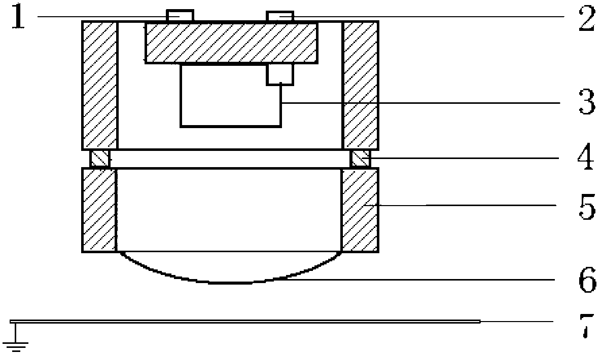
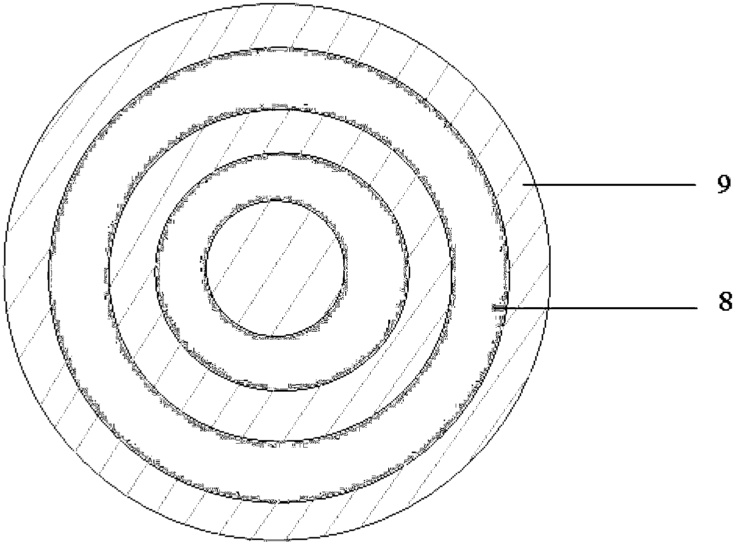
[0021] Such as figure 1 The manufacturing device of a kind of continuum electron source shown, described device is to apply an electron beam scattering film under electron gun, and described film is the Kapton film 9 that one side is coated with aluminum layer, and the other side is coated with concentric silver ring 8 ;
[0022] The diameter of the Kapton film 9 is 50 mm, and the thickness is 7.5 μm; the thickness of the aluminum layer is 100 nm; the width of the concentric silver ring is 10 mm, and the thickness is 0.2 μm, and the distance between two adjacent concentric silver rings 8 is 1 mm;
[0023] Described concentric silver ring 8 is one or more layers, between the different layers of same silver ring, width decreases successively from bottom to top, and the concentric silver ring width of the bottom layer is 10mm;
[0024] Open a hole with a diameter of 50mm on a 300×300mm aluminum disk, install the electron beam scattering film on the hole, and install the aluminum...
PUM
| Property | Measurement | Unit |
|---|---|---|
| Diameter | aaaaa | aaaaa |
Abstract
Description
Claims
Application Information
 - R&D
- Intellectual Property
- Life Sciences
- Materials
- Tech Scout
- Unparalleled Data Quality
- Higher Quality Content
- 60% Fewer Hallucinations
Browse by: Latest US Patents, China's latest patents, Technical Efficacy Thesaurus, Application Domain, Technology Topic, Popular Technical Reports.
© 2025 PatSnap. All rights reserved.Legal|Privacy policy|Modern Slavery Act Transparency Statement|Sitemap|About US| Contact US: help@patsnap.com


