A Lateral Power Device with High-k Insulation Region

A technology for lateral power devices and insulating regions, which is applied in the fields of semiconductor devices, semiconductor/solid-state device manufacturing, electrical components, etc., to achieve the effects of simple process, optimized surface electric field, and improved value of merit of drift region concentration

Active Publication Date: 2016-01-20
NANJING UNIV OF POSTS & TELECOMM INST AT NANJING CO LTD
View PDF3 Cites 0 Cited by
  • Summary
  • Abstract
  • Description
  • Claims
  • Application Information

AI Technical Summary

Problems solved by technology

The application of this structure in lateral power devices has not been reported

Method used


Image

  • A Lateral Power Device with High-k Insulation Region
  • A Lateral Power Device with High-k Insulation Region
  • A Lateral Power Device with High-k Insulation Region

Examples


Embodiment Construction

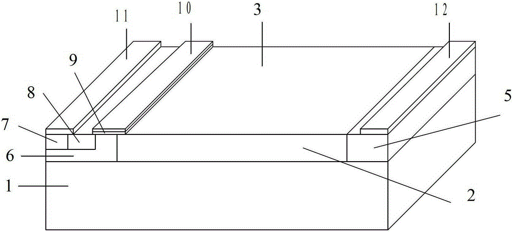
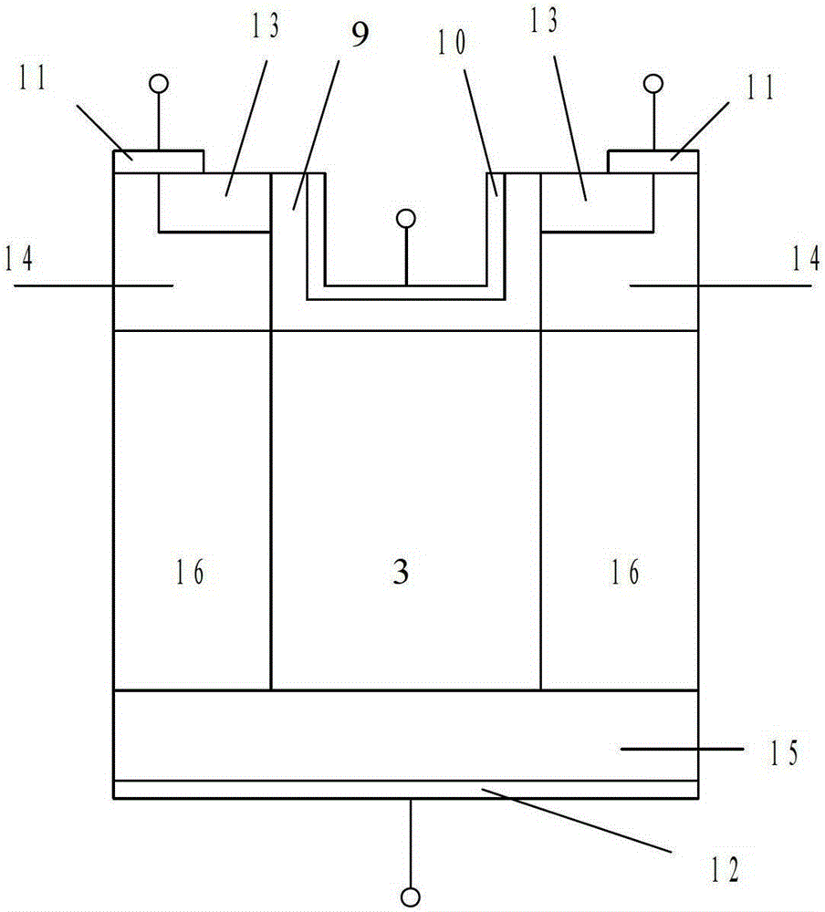
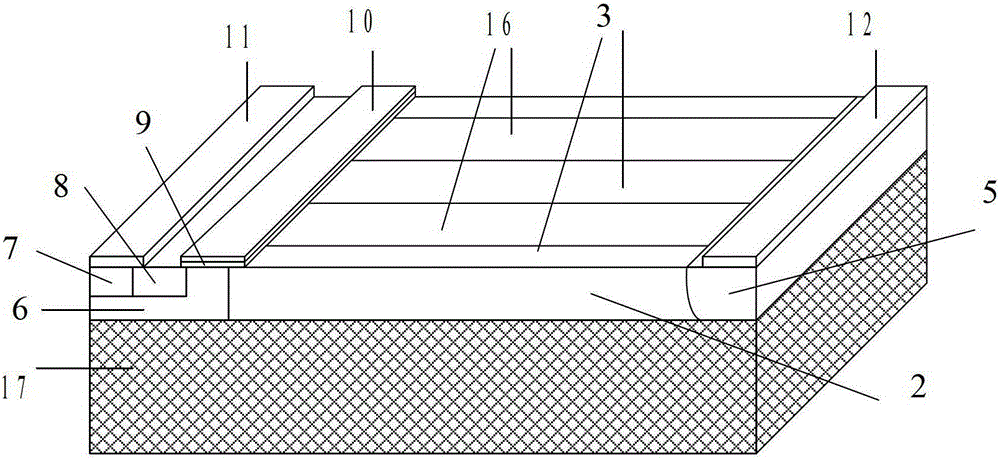
[0029] Figure 5 It is a three-dimensional view of one of the lateral power devices with a high-K insulating region provided by the present invention, and its process flow. As can be seen from the figure, it is to etch trenches with corresponding patterns on the epitaxial layer 2, and then fill the trenches with an insulating material with a high dielectric constant, thereby forming alternately arranged N-type semiconductor regions 3 and high K insulator region 4. Next, a semiconductor body region 6, a semiconductor drain region 5, a semiconductor source region 8 and a semiconductor body contact region 7 in the semiconductor body region, a gate oxide layer 9, a gate metal 10, and a source metal are formed in the epitaxial layer using a conventional LDMOS process. 11, Drain metal 12.

[0030] In the design process, according to the specific situation, certain flexible designs can be carried out under the condition that the basic structure remains unchanged, such as:

[0031]...


PUM


Abstract

The invention provides a lateral power device with a high-K insulating region, which introduces an insulating pillar region with a high dielectric constant inside the drift region of the power device, and the high-K insulating region and the N-type pillar region are alternately arranged , the insulating column region extends to the interior of the semiconductor body region. The insulating region with a high dielectric constant has the effect of reducing the field. By increasing the dielectric constant of the insulating column region, the surface electric field distribution and the optimal concentration of the drift region can be optimized, thereby improving the withstand voltage and conduction characteristics of the device. . The lateral diffused field effect transistor LDMOS, lateral PN diode, or lateral insulated gate bipolar transistor LIGBT manufactured with this structure has the advantages of high breakdown voltage, low conduction resistance, simple process, and low cost.

Description

technical field [0001] The invention belongs to the technical field of semiconductor power devices, and particularly relates to lateral power devices for high-power and high-voltage applications, such as lateral diffusion field effect transistors LDMOS, lateral PN diodes, lateral insulated gate bipolar transistors LIGBT, and the like. Background technique [0002] As we all know, in the design of lateral high-voltage power devices, factors such as breakdown voltage, on-resistance, device size, and manufacturing cost must be considered comprehensively. Usually, the improvement of performance on the one hand often leads to the reduction of performance on the other hand, especially when the breakdown voltage is increased, the on-resistance often increases at the same time. Therefore, how to obtain the compromise between the breakdown voltage and the on-resistance has always been a hot topic of research by experts and scholars. [0003] The basic structure of SOI lateral power ...

Claims


Application Information

Patent Timeline
Patent Type & Authority Patents(China)
IPC IPC(8): H01L29/78H01L29/06H01L21/336
Inventor 郭宇锋姚佳飞
Owner NANJING UNIV OF POSTS & TELECOMM INST AT NANJING CO LTD
Why Eureka
Try Eureka