Germanium (Ge) base tri-gate device and manufacturing method thereof

A device, germanium-based technology, applied in the structural form and manufacturing field of germanium-based (Ge) tri-gate (Tri-Gate) transistors, can solve problems such as difficult to control oxidation time, cumbersome operation, and influence on experimental efficiency, and achieve reduction of oxygen The effects of vacancy defects, increased dielectric constant, and simple preparation process

Inactive Publication Date: 2013-07-24
NANJING UNIV +1
View PDF5 Cites 4 Cited by
  • Summary
  • Abstract
  • Description
  • Claims
  • Application Information

AI Technical Summary

Problems solved by technology

However, both of these two preparation processes have obvious deficiencies. The oxidation step of the traditional tube furnace is to first raise the temperature inside the tube to the required value (>400°C), and then push the sample into the furnace tube for oxidation. to take out the sample, and finally to cool down
The whole process takes a long time (>2h), which affects the efficiency of the experiment. The most important thing is that it is difficult to control the oxidation time, because germanium is easily oxidized, and the germanium oxide passivation layer formed by this method is usually thick (>2nm), so it is very difficult to Conducive to the further reduction of gate oxide thickness
However, the method of using electron cyclotron resonance (ECR) plasma oxidation is cumbersome, time-consuming, power-consuming, expensive and takes up space, and has very large restrictions on production conditions, so this method is not suitable for application in actual production.

Method used


Image

  • Germanium (Ge) base tri-gate device and manufacturing method thereof
  • Germanium (Ge) base tri-gate device and manufacturing method thereof
  • Germanium (Ge) base tri-gate device and manufacturing method thereof

Examples


Embodiment Construction

[0025] In order to better understand the technical content of the present invention, specific embodiments are described below in conjunction with the accompanying drawings.

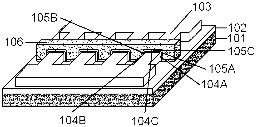
[0026] figure 1 It is a schematic diagram of the overall structure of a high-performance Ge-based tri-gate device. The germanium-based tri-gate device includes a single crystal silicon substrate 101, a silicon dioxide insulating layer 102, a single crystal germanium body 103, a germanium oxide transition layer 104A, 104B, 104C, a gate dielectric layer 105A, 105B, 105C and a gate electrode 106 A silicon dioxide insulating layer is formed on a single crystal silicon substrate, a single crystal germanium body is formed on the silicon dioxide insulating layer, and a germanium oxide transition layer is formed on three sides of the single crystal germanium body and surrounds the single crystal germanium body. On three sides, the gate dielectric layer is formed on the germanium oxide transition layer and surrounds...


PUM

PropertyMeasurementUnit
Thicknessaaaaaaaaaa
Thicknessaaaaaaaaaa

Abstract

The invention provides a germanium (Ge) base tri-gate device and a manufacturing method thereof. The Ge base tri-gate device mainly comprises four functional layers including a germanium (GOI) substrate on an insulating layer, a germanium oxide transition layer, a grid electrode dielectric layer and a gate electrode layer. The high-quality and ultrathin germanium oxide transition layer achieved after ozone post-oxidation process and the high-quality grid electrode dielectric layer improved after the ozone post-oxidation are key layers to achieve high performance. The step of removing Ge, with poor quality (large surface roughness and high impurity content), on the surface of a Ge body through sacrificial oxidation process is a key step to achieve the high performance. The manufacturing process mainly comprises the step of depositing and etching on the germanium (GOI) substrate on the insulating layer to form the functional layers. According to the Ge base tri-gate device, efficiency is high, power consumption is low, the manufacturing method is simple, and the device is suitable for being widely used to actual production.

Description

Technical field [0001] The invention belongs to the technical field of semiconductor integrated circuits and their manufacturing, and proposes a structure and manufacturing method of a germanium-based (Ge) tri-gate (Tri-Gate) transistor. Background technique [0002] With the development of integrated circuit technology, for the performance of integrated circuits, Tri-gate devices have higher switching ratios and excellent short-channel effect control capabilities compared with planar devices and two-dimensional devices. Outstanding advantages are gradually being used in the manufacture of integrated circuits. Compared with traditional silicon-based tri-gate devices, the outstanding advantage of germanium-based tri-gate devices is that it has much higher electron and hole mobility than silicon, which can greatly increase the driving current of the transistor. Secondly, the band gap of germanium (about 0.66eV) is also narrower than that of silicon (1.1eV), which also allows its o...

Claims


Application Information

Patent Timeline
IPC IPC(8): H01L29/78H01L29/423H01L21/336H01L21/28
Inventor 赵毅孙家宝施毅赵杰董晓宇
Owner NANJING UNIV
Why Eureka
Try Eureka