
Manufacturing method of self-aligned insulated gate bipolar transistor

A technology of bipolar transistors and manufacturing methods, which is applied in semiconductor/solid-state device manufacturing, electrical components, circuits, etc., can solve the problem that the size of the emission area of ​​lithography precision cannot be reduced, and achieve the reduction of strict alignment times of lithography, and the device Effect of small structure size and reduced power consumption

Active Publication Date: 2013-07-24
中国东方电气集团有限公司 +1
View PDF4 Cites 13 Cited by
  • Summary
  • Abstract
  • Description
  • Claims
  • Application Information

AI Technical Summary

Problems solved by technology

[0008] In order to overcome the problem that the size of the emitter region cannot be reduced to the ideal size due to the limitation of photolithography precision in the existing method of manufacturing planar gate bipolar transistors, a kind of automatic method suitable for planar gate bipolar transistors is specially proposed. Aligned Insulated Gate Bipolar Transistor Fabrication Method

Method used


Image

  • Manufacturing method of self-aligned insulated gate bipolar transistor
  • Manufacturing method of self-aligned insulated gate bipolar transistor
  • Manufacturing method of self-aligned insulated gate bipolar transistor

Examples


Embodiment Construction

[0069] A method for manufacturing a self-aligned insulated gate bipolar transistor, comprising the steps of:

[0070] A. A crystalline silicon substrate of the first conductivity type is provided as the base region of the first conductivity type;

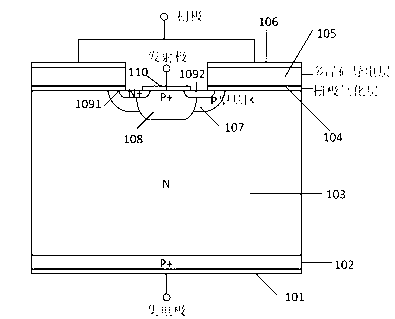
[0071] There are two types of conductivity, one is N-type conductivity, and the other is P-type conductivity. The first conductivity type mentioned here is any one of them, and the second conductivity type is another one. The base region of the first conductivity type is located at the carrier diffusion region 103 .

[0072] B. making a first insulating layer on the front side of the crystalline silicon substrate;

[0073] Here, the first insulating layer refers to the first insulating layer to be processed. The position of the first insulating layer is at the gate oxide layer 104 . Available materials include insulating materials such as silicon oxide, silicon nitride, and aluminum oxide.

[0074] C. Depositing a polysilicon gat...


PUM

PropertyMeasurementUnit
Thicknessaaaaaaaaaa

Abstract

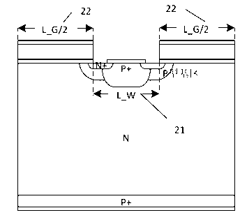
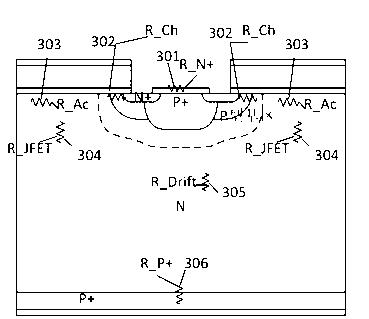
The invention relates to semiconductor devices in the technical field of power electronics, and particularly relates to a manufacturing method of a self-aligned insulated gate bipolar transistor applicable to a planar gate bipolar transistor. The manufacturing method adopts a window as a mask and realizes manufacturing of a first conduction type doped region of one side 431 of the window by first-time inclined implantation. The manufacturing method provides a technology which does not need photoetching and can control the width of an N+ emitter region, and further provides a set of full-self-aligned method for manufacturing an IGBT (Insulated Gate Bipolar Transistor) device. Compared with the traditional process, the method has the advantages that due to reduction of strict aligning times of photoetching, the width of a P-type base region can be effectively reduced, the concentration of minority carriers under a gate is increased, the conductivity modulation effect is improved, and the influence of a JEFT (Junction Field Effect Transistor) is reduced, so that the power consumption of the IGBT is reduced; and due to reduction of the strict aligning times of photoetching, the manufacturing cost is effectively reduced and the fault rate is reduced.

Description

technical field [0001] The invention relates to semiconductor devices in the technical field of power electronics, in particular to a method for manufacturing a self-aligned insulated gate bipolar transistor suitable for planar gate bipolar transistors. Background technique [0002] IGBT (Insulated Gate Bipolar Transistor, Insulated Gate Bipolar Transistor) has been developed to the sixth generation technology since it came out in the 1980s, and related products are widely used in inverters, electric vehicles, railways, home appliances and other fields. For the planar IGBT (as shown in Figure 1), in order to improve its performance and market competitiveness, it is necessary to achieve high withstand voltage, high current and low power consumption on the basis of its advantages of relatively simple preparation and relatively low cost. Target. [0003] The withstand voltage of the IGBT depends on the doping concentration, the thickness of the drift region, and the lifetime o...

Claims


Application Information

Patent Timeline
IPC IPC(8): H01L21/331H01L21/266
Inventor 胡强张世勇樱井建弥
Owner 中国东方电气集团有限公司
Learn More