Display, thin film transistor array substrate and manufacturing process thereof

A technology of thin film transistors and array substrates, applied in the field of liquid crystal displays, can solve problems such as high complexity, low yield, and many process steps, and achieve the effects of reducing complexity, improving production efficiency, and simplifying process steps

Active Publication Date: 2016-06-08
BOE TECH GRP CO LTD
View PDF8 Cites 0 Cited by
  • Summary
  • Abstract
  • Description
  • Claims
  • Application Information

AI Technical Summary

Problems solved by technology

[0006] The fabrication of the TFT thin film transistor array substrate with this structure requires eight mask exposure processes to form the gate electrode 102, the active layer 104, the source / drain electrodes (105, 106), the protective layer 107, the black matrix 108, and the color filter. film 109 (the three primary colors require a total of three mask exposure processes) and pixel electrodes 110, and a gate insulating layer 103 and a protective layer 107 are also provided at the same time, so that the entire process has many steps, high complexity, and low yield

Method used


Image

  • Display, thin film transistor array substrate and manufacturing process thereof
  • Display, thin film transistor array substrate and manufacturing process thereof
  • Display, thin film transistor array substrate and manufacturing process thereof

Examples


Embodiment Construction

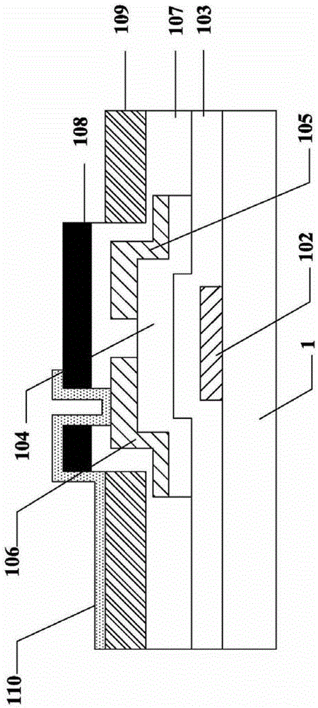
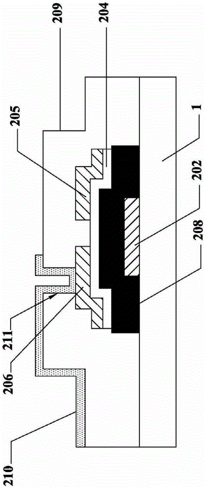
[0032] The thin film transistor array substrate of the present invention uses black resin as the insulating layer of the gate, and simultaneously serves as a black matrix for dividing sub-pixels. Because the gate insulating layer of the black resin material is thick and the dielectric constant is high, the performance of the thin film transistor will be reduced, so the technical solution of the present invention is also doped with a small amount of metal powder (such as silver powder, copper powder, etc.) in the black resin, In order to reduce its dielectric constant and ensure the good performance of the thin film transistor.

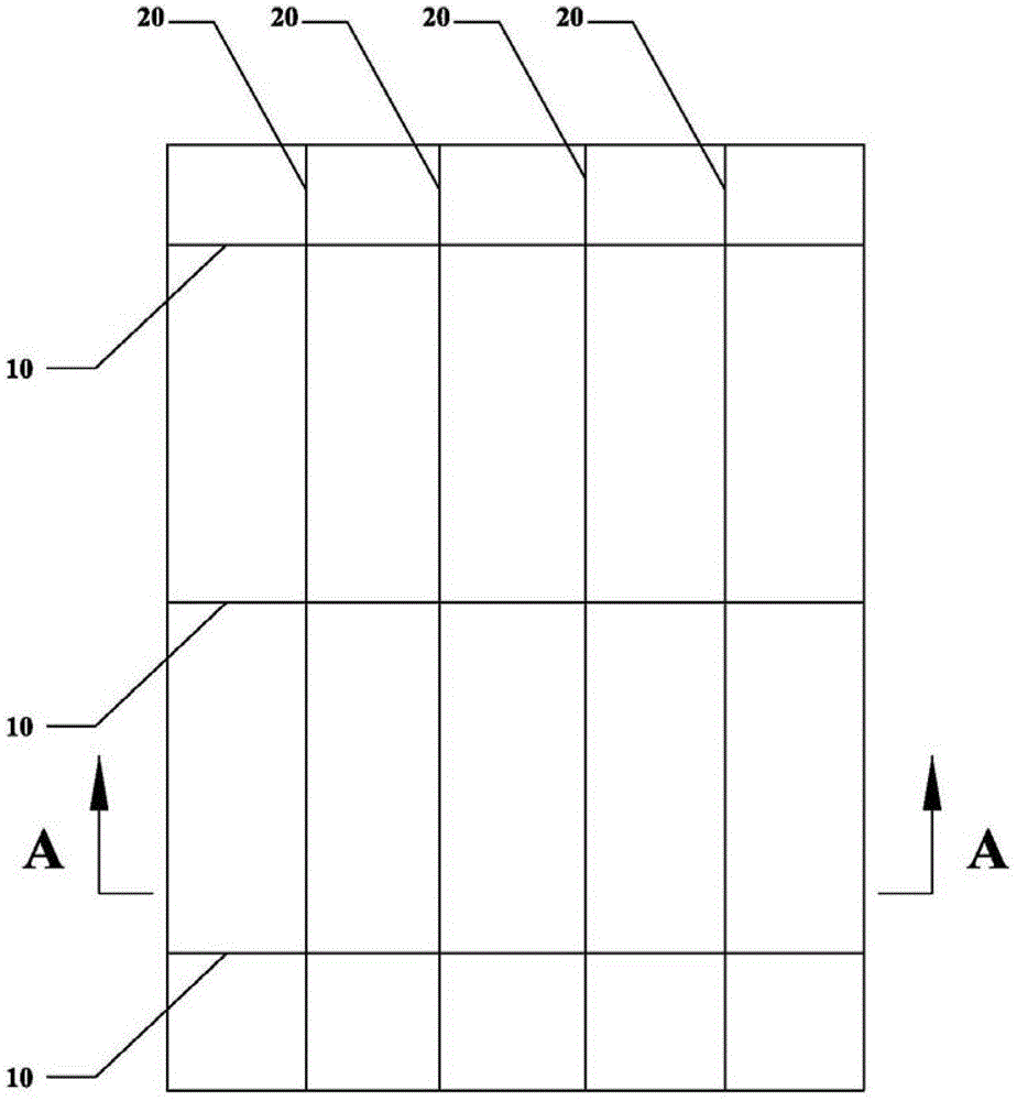
[0033] Such as figure 2 , image 3 As shown, the embodiment of the thin film transistor array substrate of the present invention includes gate lines 10, data lines 20, and pixel electrodes 210 formed in the pixel regions defined by the gate lines 10 and data lines 20, and also includes:

[0034] a gate electrode 202 formed on the substrate 1;

[00...


PUM


Abstract

The invention relates to a display, a thin film transistor array substrate and a manufacturing process thereof. Wherein, the thin film transistor array substrate includes: a gate electrode, an active layer, and the gate electrode and the active layer are separated by a black matrix; a source electrode, a drain electrode and a channel; a color filter layer, and a pixel electrode. The display of the present invention includes the thin film transistor array substrate of the present invention. The manufacturing process of the thin film transistor array substrate of the present invention includes forming the pattern of the gate line and the gate electrode on the substrate; forming the pattern of the black matrix; forming the pattern of the active layer and the source / drain electrode; forming the pattern of the color filter layer; A pattern of pixel electrodes is formed. The thin film transistor array substrate of the present invention omits the gate insulating layer and the protective layer, and avoids two plasma gas phase film forming processes, significantly shortens the process time and reduces the complexity of the process; meanwhile, the thickness of the substrate is effectively thinned. The manufacturing process of the thin film transistor array substrate of the present invention effectively reduces the times of film formation and shortens the process time.

Description

technical field [0001] The invention relates to the technical field of liquid crystal displays, in particular to a display, a thin film transistor array substrate and a manufacturing process thereof. Background technique [0002] Thin Film Transistor Liquid Crystal Display (TFT-LCD) has the advantages of small size, low power consumption, and no radiation, and occupies a dominant position in the current flat panel display market. For TFT-LCD, the thin film transistor array substrate and manufacturing process determine its product performance, yield and price. [0003] The traditional TFT-LCD consists of a TFT thin film transistor array substrate and another color filter substrate (ColorFilter). On the TFT thin film transistor array substrate are formed control switching thin film transistors and pixel electrodes, and on the color filter substrate are formed red, green, blue light filter layers and common electrodes. The liquid crystal molecules are sandwiched between the t...

Claims


Application Information

Patent Timeline
Patent Type & Authority Patents(China)
IPC IPC(8): H01L27/12H01L29/786H01L21/77G02F1/136
CPCG02F1/136209G02F1/1368H01L29/4908H01L27/1237H01L27/1248G02F1/136222H01L27/124H01L27/1262H01L33/58
Inventor 牛菁
Owner BOE TECH GRP CO LTD
Why Eureka
Try Eureka