Silicon substrate niobium nitride film superconducting material and preparing method thereof

A technology of superconducting material and niobium nitride, which is applied in the manufacturing/processing of superconducting devices, superconducting parts, metal material coating process, etc., can solve the problem of reducing the superconducting properties of NbN thin films and the large lattice mismatch of crystal structure. , there are gaps in superconducting performance, etc.

Inactive Publication Date: 2013-06-19
SUZHOU UNIV
View PDF4 Cites 3 Cited by
  • Summary
  • Abstract
  • Description
  • Claims
  • Application Information

AI Technical Summary

Problems solved by technology

However, these materials have two major disadvantages: one is that the crystal structure and lattice mismatch are still relatively large; the other is that the constituent elements of these materials will reduce the superconducting properties of NbN films if they diffuse into the NbN film
Therefore, there is still a gap betwee

Method used


Image

  • Silicon substrate niobium nitride film superconducting material and preparing method thereof
  • Silicon substrate niobium nitride film superconducting material and preparing method thereof
  • Silicon substrate niobium nitride film superconducting material and preparing method thereof

Examples


Embodiment Construction

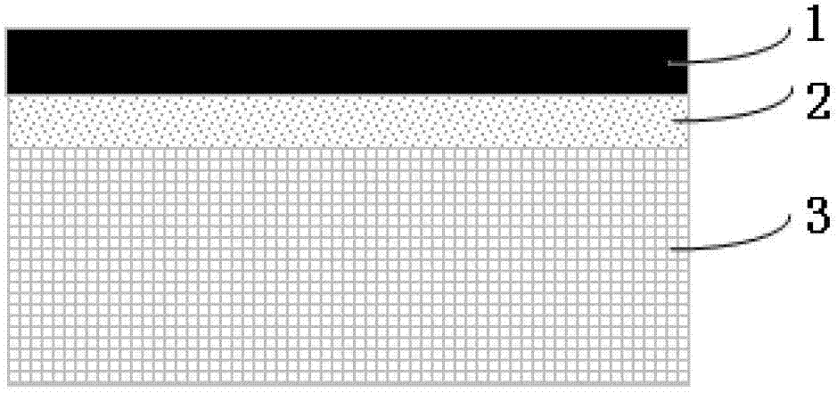
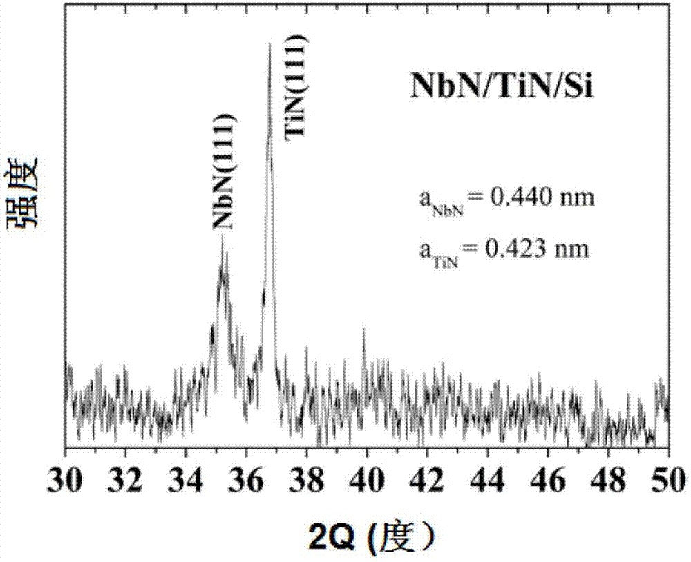
[0028] As mentioned in the background technology, the existing Si-based NbN thin-film superconducting materials still lack suitable transition layer materials, and it is impossible to obtain thin-film superconducting materials with good lattice matching between Si crystal and NbN layer and excellent superconducting properties. To a certain extent, the application field of Si-based NbN thin film superconducting materials is limited.

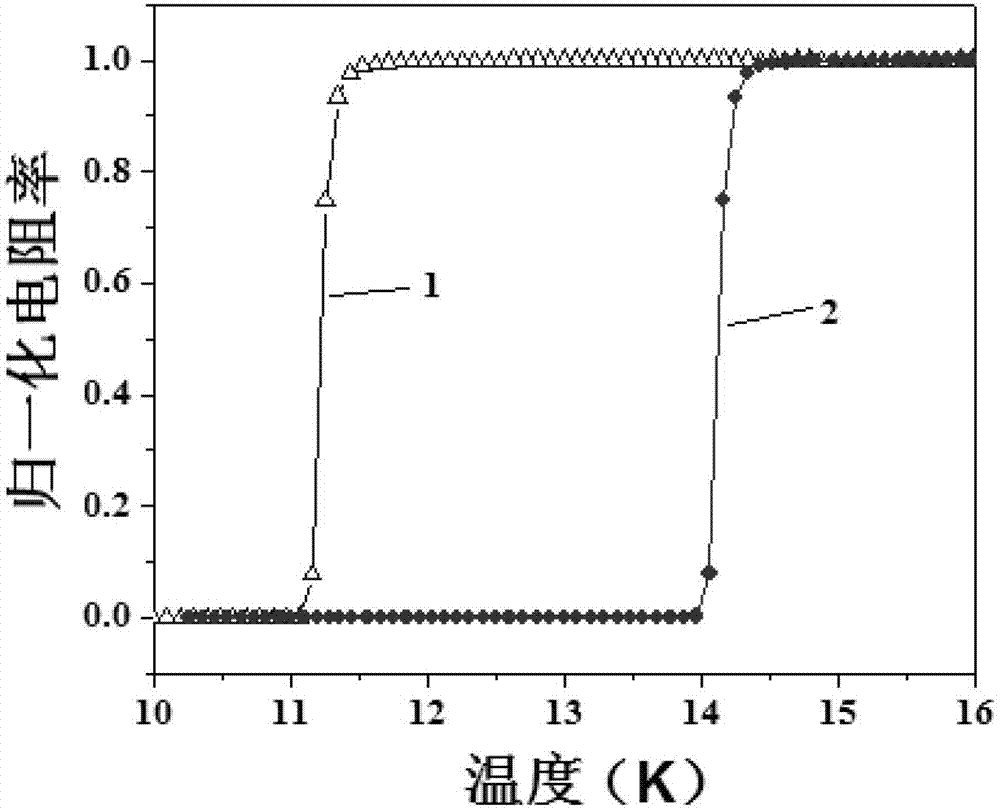
[0029] Therefore, the present invention proposes a new Si-based NbN thin film superconducting material. The Si-based NbN thin film superconducting material uses TiN as a transition layer. Since TiN and NbN both belong to the face-centered cubic structure, and the lattice mismatch is small, Therefore, the use of the TiN transition layer greatly reduces the thickness of the interfacial distortion layer in the NbN film, while the crystallinity of NbN is improved; and NbTiN itself is a T c For higher superconducting materials, even if the two elements...


PUM


Abstract

The invention discloses a silicon substrate niobium nitride film superconducting material. The silicon substrate niobium nitride film superconducting material comprises a Si substrate, a TiN transitional layer and an NbN layer. An NbN film is directly arranged on the Si substrate in a growth mode to cause a big lattice mismatch degree so that a non-superconducting interface distortion layer with a certain thickness can exist in the NbN film, and superconducting performance of the NbN film is severely reduced. The TiN transitional layer and the NbN layer are of a face-centred cubic structure, the lattice mismatch degree is small, the TiN transitional layer is used for greatly reducing the interface distortion layer thickness of the NbN film, NbN crystallinity is simultaneously improved, and superconducting performance is improved accordingly. The NbTiN is high-Tc superconducting materials, and even if two elements including Ti and N in the TiN enter the NbN film, the Ti and the N are not reduced, and the superconducting performance of the Ti and the N is improved. The invention further provides a manufacturing method of the silicon substrate niobium nitride film superconducting material.

Description

technical field [0001] The invention relates to the field of superconducting material production, in particular to a silicon-based niobium nitride thin film superconducting material and a production method thereof. Background technique [0002] NbN (niobium nitride) thin film is the core material of various superconducting devices, such as superconducting tunnel junction (Superconducting tunnel junction), hot electron bolometer (HEB, Hot Electron Bolometer), superconducting single photon detection device (SSPD) , Superconducting Single Photon Detector), etc. Usually, NbN thin films are prepared on MgO single crystal substrates by vacuum magnetron sputtering technology. The main consideration is that the lattice mismatch between NbN and MgO is small (~4%), and the grown NbN thin films have good superconducting properties. . However, the price of MgO single crystal substrate is high, the micro-nano processing technology of subsequent devices is immature, and the loss of devi...

Claims


Application Information

Patent Timeline
IPC IPC(8): H01L39/12H01L39/24C23C14/06C23C14/35
Inventor 苏晓东张婧娇郑磊
Owner SUZHOU UNIV
Why Eureka
Try Eureka