Storage Elements and Storage Devices

A storage element and storage layer technology, applied in the direction of electrical components, information storage, static memory, etc., to achieve the effects of reducing energy consumption, high reliability, and avoiding operating errors

Active Publication Date: 2017-06-16
SONY CORP
View PDF4 Cites 0 Cited by
  • Summary
  • Abstract
  • Description
  • Claims
  • Application Information

AI Technical Summary

Problems solved by technology

Also, because this current value is proportional to the component volume, scaling is possible

Method used


Image

  • Storage Elements and Storage Devices
  • Storage Elements and Storage Devices
  • Storage Elements and Storage Devices

Examples


Embodiment Construction

[0049] Embodiments of the present invention will be described in the following order.

[0050]

[0051]

[0052]

[0053]

[0054]

[0055]

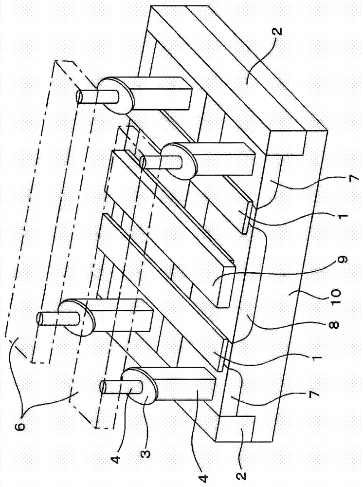
[0056] First, the structure of a storage device according to an embodiment of the present invention will be described.

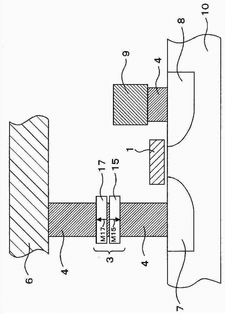
[0057] figure 1 with figure 2 Schematic diagrams of storage devices according to the embodiments are shown respectively. figure 1 is a stereogram, and figure 2 is a sectional view.

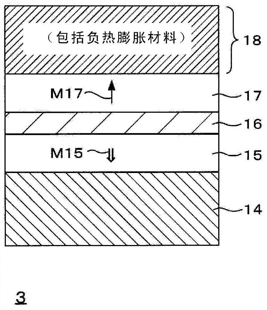
[0058] Such as figure 1 As shown, in the memory device according to the embodiment, the memory element 3 including ST-MRAM capable of retaining information depending on the magnetization state is arranged in two kinds of address interconnections (eg, sub-lines and bit lines) perpendicular to each other. near the point of intersection.

[0059] In other words, drain region 8 , source region 7 , and gate electrode 1 constituting a selection transistor for selecting each memory device are formed in semiconductor substrate ...


PUM


Abstract

The present invention provides a memory element and a memory device. The memory element includes a layered structure and a layer of negative thermal expansion material. The layered structure includes a storage layer, a magnetization fixed layer, and an intermediate layer. The storage layer has magnetization perpendicular to the film plane in which the direction of magnetization changes according to information, and includes a magnetic layer having a positive magnetostriction constant. The direction of magnetization is changed by applying a current along the stacking direction of the layered structure to record information in the storage layer. The magnetization fixed layer has magnetization perpendicular to the film surface, and becomes the basis of information stored in the storage layer. The intermediate layer is formed of a non-magnetic material, and is provided between the storage layer and the magnetization fixed layer.

Description

technical field [0001] The present invention relates to a storage element and a storage device having a plurality of magnetic layers and recording using spin-magnetic moment magnetization switching. Background technique [0002] With the rapid development of various information devices ranging from mobile terminals to large-capacity servers, further improvements in performance, such as higher integration, speed, etc. elevated and lower power consumption. Specifically, semiconductor nonvolatile memory has been significantly advanced, and flash memory has been widely used as a large-capacity file storage at a speed that can replace hard disks. In addition, the development of FeRAM (Ferroelectric Random Access Memory), MRAM (Magnetic Random Access Memory), PCRAM (Phase Change Random Access Memory), etc. has been advanced as a substitute for the current general NOR flash memory, DRAM, etc. Use it for code storage or working memory. Some of these devices have already been put ...

Claims


Application Information

Patent Timeline
Patent Type & Authority Patents(China)
IPC IPC(8): H01L43/08H01L43/02H01L27/22G11C11/16
CPCG11C11/161G11C11/1675H10B61/22H10N50/85H10N50/10H01L29/82
Inventor 山根一阳细见政功大森广之别所和宏肥后丰浅山彻哉内田裕行
Owner SONY CORP
Why Eureka
Try Eureka