RF LDMOS (ratio frequency laterally diffused metal oxide semiconductor) device and manufacture method of RF LDMOS device
A device, N-type technology, applied in semiconductor/solid-state device manufacturing, semiconductor devices, electrical components, etc., can solve problems such as complex manufacturing process, and achieve the effects of simple device manufacturing process, reduced metal deposition, and high breakdown voltage
- Summary
- Abstract
- Description
- Claims
- Application Information
AI Technical Summary
Problems solved by technology
Method used
Image
Examples
Embodiment 1
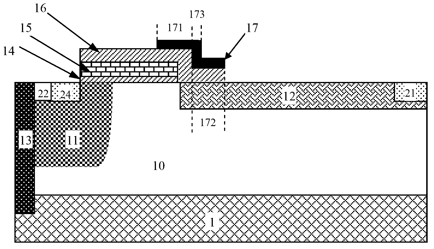
[0046] The structure of RF LDMOS device is as Figure 4 shown. An N-type drain end lightly doped drift region 12 is formed on the right part of the P epitaxy 10, and a gate oxide 14 is formed on the P epitaxy 10 on the left side of the N-type drain end lightly doped drift region 12, above the gate oxide 14 A polysilicon gate 15 is formed, a dielectric layer 16 is formed on the top of the polysilicon gate 15, on the side and on the left part of the lightly doped drift region 12 of the N-type drain, and a Faraday shield is formed on the right part of the dielectric layer 16. shield) 17, the Faraday shield 17 is a single-layer metal layer, the single-layer metal layer includes a polysilicon portion 171, a drift portion 172, and a vertical portion 173, the vertical portion 173 is on the right side of the polysilicon gate 15, and the upper end of the vertical portion 173 It communicates with the right end of the polysilicon part 171, the lower end of the vertical part 173 communic...
Embodiment 2
[0050] Based on Embodiment 1, the structure of the RF LDMOS device is as follows Figure 4 shown. A P well 11 is formed on the left part of the P epitaxy 10, and an N-type drain terminal lightly doped drift region 12 is formed on the right part of the P epitaxy 10, and the P well 11 and the N-type drain terminal lightly doped drift region are formed. 12 no contact;
[0051] An N-type source terminal heavily doped region 24 is formed on the upper part of the P well 11;
[0052] An N-type drain heavily doped region 21 is formed in the right part of the N-type drain lightly doped drift region 12;
[0053] The N-type impurity concentration of the N-type source heavily doped region 24 and the N-type drain heavily doped region 21 is greater than the N-type impurity concentration of the N-type drain lightly doped drift region 12;
[0054] Above the P well 11 on the right side of the N-type source heavily doped region 24, and above the P epitaxy 10 between the P well 11 and the N-t...
Embodiment 3
[0056] The manufacturing method of the RF LDMOS device described in embodiment one, comprises the following steps:
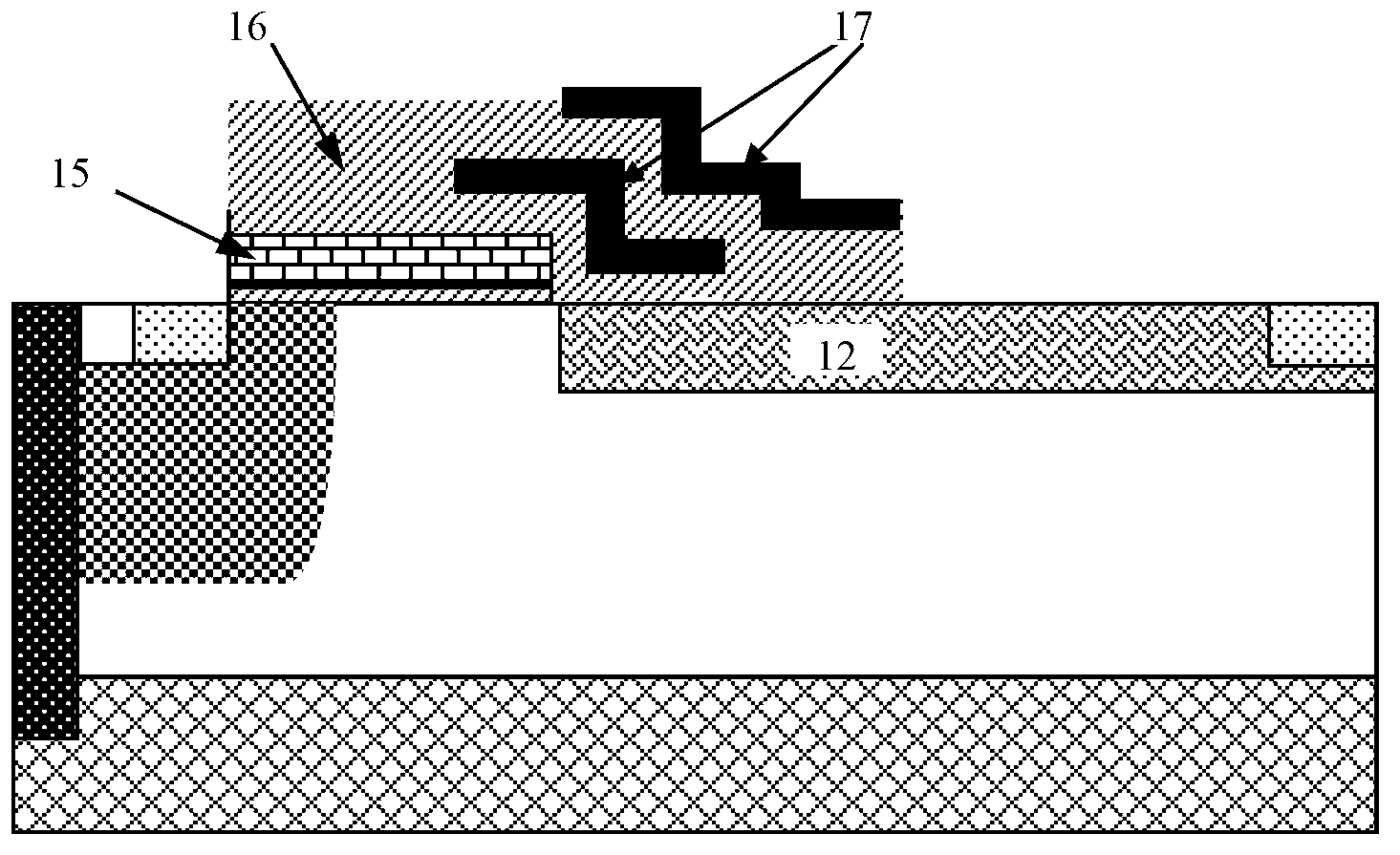
[0057] 1. Form gate oxide 14, polysilicon gate 15, N-type drain lightly doped drift region 12, N-type drain lightly doped drift region 12 is formed on the right part of P epitaxy 10, gate oxide 14 is formed on N-type drain On the P epitaxy 10 on the left side of the lightly doped drift region 12, a polysilicon gate 15 is formed on the gate oxide 14, as Figure 5 shown;
[0058] two. A layer of silicon oxide 16 is integrally deposited on the silicon wafer, such as Image 6 shown; preferably, the thickness of the layer of silicon oxide is 1000-4000 angstroms;
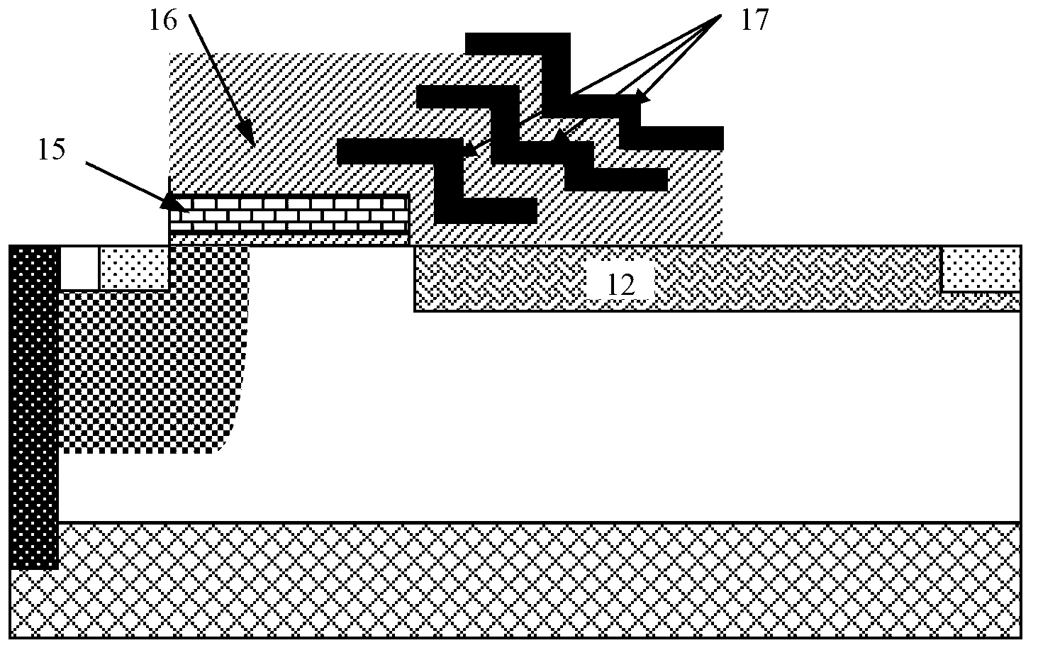
[0059] three. By photolithography, a groove is formed in the silicon oxide above the left part of the lightly doped drift region of the N-type drain, and the depth of the groove is smaller than the thickness of the layer of silicon oxide 16, such as Figure 7 shown; preferably, the width of the trench ...
PUM
| Property | Measurement | Unit |
|---|---|---|
| thickness | aaaaa | aaaaa |
| depth | aaaaa | aaaaa |
| breakdown voltage | aaaaa | aaaaa |
Abstract
Description
Claims
Application Information
 - Generate Ideas
- Intellectual Property
- Life Sciences
- Materials
- Tech Scout
- Unparalleled Data Quality
- Higher Quality Content
- 60% Fewer Hallucinations
Browse by: Latest US Patents, China's latest patents, Technical Efficacy Thesaurus, Application Domain, Technology Topic, Popular Technical Reports.
© 2025 PatSnap. All rights reserved.Legal|Privacy policy|Modern Slavery Act Transparency Statement|Sitemap|About US| Contact US: help@patsnap.com


