Method for measuring concentration of germanium or/and tin impurity in crystalline silicon
A technology of impurity concentration and measurement method, which is applied in the field of measurement of germanium or/and tin impurity concentration in crystalline silicon, can solve problems such as difficulty in detection of impurity concentration of germanium-tin master alloy, and achieve complex detection methods, cost reduction, and small deviation Effect
- Summary
- Abstract
- Description
- Claims
- Application Information
AI Technical Summary
Problems solved by technology
Method used
Image
Examples
Embodiment 1
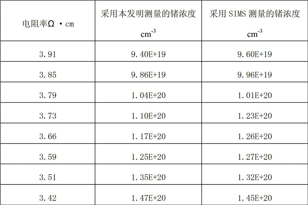
[0030] Embodiment 1. The measuring method of germanium or / and tin impurity concentration in crystalline silicon, comprises the steps:
[0031] 1. Add 0.005 grams of boron powder with a purity of 6N-7N and 2000 grams of germanium with a purity of 5N-7N into 150,000 grams of solar-grade polysilicon raw materials, and form a silicon melt through the Czochralski single crystal manufacturing method (CZ method). Body, under the protective atmosphere of argon, the P-type germanium-containing master alloy silicon rod is prepared;
[0032] 2. Cut the germanium-containing master alloy silicon rod in step 1 into germanium-containing master alloy silicon wafers with a thickness of 3 mm by internal circle cutting or multi-wire cutting, and then use the solar-grade silicon material cleaning process to clean the germanium-containing master alloy silicon wafers. surface cleaning;
[0033] 3. Utilize the four-probe method to measure the resistivity ρ of the germanium-containing master alloy s...
Embodiment 2
[0048] Embodiment 2. The measuring method of germanium or / and tin impurity concentration in crystalline silicon, comprises the steps:
[0049] 1. Add 0.005 grams of phosphorus with a purity of 6N-7N and 2000 grams of tin with a purity of 6N-7N into 150,000 grams of solar-grade polysilicon raw materials, and form a silicon melt through the Czochralski single crystal manufacturing method (CZ method). Body, under the protective atmosphere of argon, the N-type tin-containing master alloy silicon rods were prepared;
[0050] 2. Cut the tin-containing master alloy silicon in step 1 into a tin-containing master alloy silicon wafer with a thickness of 1mm by means of internal circle cutting, multi-wire cutting, etc., and then use a solar-grade silicon material cleaning process to clean the tin-containing master alloy Silicon wafer surface cleaning;
[0051] 3. Use the four-probe method to measure the resistivity ρ of the tin-containing master alloy silicon chip obtained in step 2, an...
PUM
| Property | Measurement | Unit |
|---|---|---|
| thickness | aaaaa | aaaaa |
| thickness | aaaaa | aaaaa |
Abstract
Description
Claims
Application Information
 - R&D
- Intellectual Property
- Life Sciences
- Materials
- Tech Scout
- Unparalleled Data Quality
- Higher Quality Content
- 60% Fewer Hallucinations
Browse by: Latest US Patents, China's latest patents, Technical Efficacy Thesaurus, Application Domain, Technology Topic, Popular Technical Reports.
© 2025 PatSnap. All rights reserved.Legal|Privacy policy|Modern Slavery Act Transparency Statement|Sitemap|About US| Contact US: help@patsnap.com


