Compound semiconductor device and method of manufacturing the same
A semiconductor and compound technology, applied in the field of compound semiconductor devices and their manufacturing, can solve problems such as difficulty in fully suppressing current collapse
- Summary
- Abstract
- Description
- Claims
- Application Information
AI Technical Summary
Problems solved by technology
Method used
Image


Examples
no. 1 approach
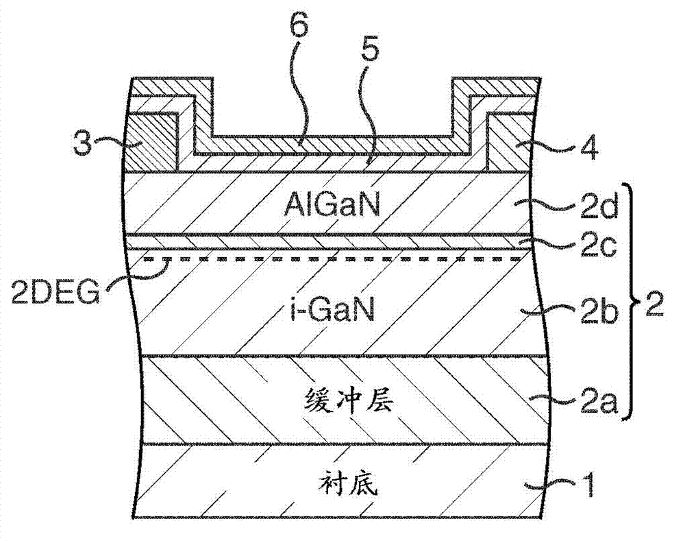
[0044] In this embodiment, a Schottky-type AlGaN / GaN HEMT is disclosed as a compound semiconductor device.
[0045] Figure 1A to Figure 1C and Figure 2A to Figure 2C is a schematic cross-sectional view showing a method of manufacturing the AlGaN / GaN HEMT according to the first embodiment in the order of processes.
[0046] First, if Figure 1A As shown, a compound semiconductor layer 2 having a compound semiconductor stack structure is formed on, for example, a semi-insulating SiC substrate 1 as a growth substrate. As the growth substrate, a SiC substrate, a sapphire substrate, a GaAs substrate, a GaN substrate, or the like can be used instead of the SiC substrate. The conductivity of the substrate can be semi-insulating or conducting.
[0047] The compound semiconductor layer 2 includes a buffer layer 2a, an electron transport layer 2b, an intermediate layer 2c, and an electron supply layer 2d.
[0048] In the completed AlGaN / GaN HEMT, during operation, a two-dimensiona...
no. 2 approach
[0079] Hereinafter, a Schottky-type AlGaN / GaN HEMT according to a second embodiment will be described. Note that the same constituent members and the like as those of the AlGaN / GaN HEMT according to the first embodiment will be denoted by the same reference numerals, and a detailed description thereof will be omitted.
[0080] Figure 4A to Figure 4C is a schematic cross-sectional view showing main processes in the method of manufacturing the AlGaN / GaN HEMT according to the second embodiment.
[0081] First, through the first embodiment of the Figure 1A to Figure 2A In the process, the opening 6a is formed in the SiON film 6, such as Figure 4A shown.
[0082] Subsequently, if Figure 4B As shown, trenches 11 are formed in SiON film 6 and electron supply layer 2d.
[0083] In more detail, photoresist is applied on the entire surface of SiON film 6 (including the upper portion of SiN film 5 exposed from opening 6a), and the photoresist is processed by photolithography. T...
no. 3 approach
[0095] Hereinafter, an MIS-type AlGaN / GaN HEMT according to a third embodiment will be described. Note that the same constituent members and the like as those of the AlGaN / GaN HEMT according to the first embodiment will be denoted by the same reference numerals, and a detailed description thereof will be omitted.
[0096] Figure 5A and Figure 5B is a schematic cross-sectional view showing main processes in the method of manufacturing the AlGaN / GaN HEMT according to the third embodiment.
[0097] First, through the first embodiment of the Figure 1A to Figure 2A In the step, an opening 6a is formed in the SiON film 6, such as Figure 5A shown.
[0098] Subsequently, if Figure 5B As shown, a gate electrode 13 is formed.
[0099] For example, Ni / Au (Ni for the lower layer and Au for the upper layer) is used as the electrode material. For forming electrodes, for example, a double-layer photoresist of an eaves structure suitable for a vapor deposition method and a lift-of...
PUM
 Abstract
Description
Claims
Application Information
 - R&D
- Intellectual Property
- Life Sciences
- Materials
- Tech Scout
- Unparalleled Data Quality
- Higher Quality Content
- 60% Fewer Hallucinations
Browse by: Latest US Patents, China's latest patents, Technical Efficacy Thesaurus, Application Domain, Technology Topic, Popular Technical Reports.
© 2025 PatSnap. All rights reserved.Legal|Privacy policy|Modern Slavery Act Transparency Statement|Sitemap|About US| Contact US: help@patsnap.com