
A metal through-type back-emitter crystalline silicon solar cell based on an n-type silicon wafer and its preparation method

A technology of crystalline silicon solar cells and back emitters, which is applied in the manufacture of circuits, electrical components, and final products. Reduce compound speed and improve the effect of unfavorable factors

Active Publication Date: 2015-08-05
ZHEJIANG JINKO SOLAR CO LTD
View PDF3 Cites 0 Cited by
  • Summary
  • Abstract
  • Description
  • Claims
  • Application Information

AI Technical Summary

Problems solved by technology

[0004] Traditional boron-doped p-type crystalline silicon solar cells have some disadvantages. First, the p-type silicon wafer itself is doped with boron, and the formation of boron-oxygen recombination pairs will cause the conversion efficiency to decay. Second, the minority carriers in the p-type silicon wafer are electrons. Recombination sensitivity caused by impurities leads to low minority carrier lifetime
In addition, traditional solar cells cover the back of the silicon wafer with all aluminum to form an aluminum back field, which will cause the battery to bend. As the thickness of the silicon wafer decreases, the curvature will become more and more serious

Method used


Image

  • A metal through-type back-emitter crystalline silicon solar cell based on an n-type silicon wafer and its preparation method

Examples


Embodiment 1

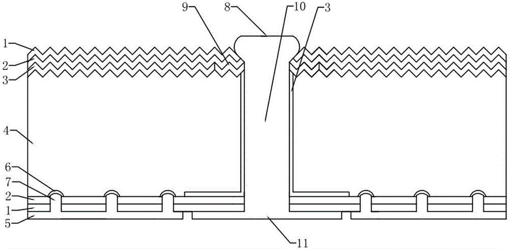
[0014] like figure 1 As shown, a metal through-type back-emitter crystalline silicon solar cell based on an n-type silicon wafer includes an n-type crystalline silicon wafer substrate 4, SiN x Film layer 1, SiO 2 Film layer 2, shallow doping n + Layer 3, p-type contact electrode 5, local contact emitter p + Layer 6, laser sintered hole 7, front contact electrode 8, heavily doped n ++ The layer 9, the through hole 10 and the n-type contact electrode 11; the n-type crystalline silicon wafer substrate 4 is a polycrystalline silicon wafer of 156×156 mm, and the resistivity is 1.5Ωcm. The specific preparation process is as follows: laser-drilling the n-type crystalline silicon wafer substrate 4 to form through holes 10 with a diameter of 160 μm, then cleaning and texturing and chemical polishing on the backside; then prefabricating fine gates on the front side of the silicon wafer substrate 4 The laser is heavily doped at the line to form a heavily doped n ++ Layer 9, the squa...

Embodiment 2

[0016] like figure 1 As shown, the metal through-type back-emitter crystalline silicon solar cell based on the n-type silicon wafer has the same structure as the first embodiment; The specific preparation process is as follows: laser-drilling the n-type crystalline silicon wafer substrate 4 to form through holes 10 with a diameter of 220 μm, then cleaning and texturing and chemical polishing on the back; then prefabricating fine gates on the front of the silicon wafer substrate 4 The laser is heavily doped at the line to form a heavily doped n ++ Layer 9, the square resistance is 45Ω / □; the non-thin gate line and the inner wall of the through hole 10 are diffused to form a surface field shallowly doped n + Layer 3, the square resistance is 85Ω / □; the edge PN junction of the silicon wafer is plasma etched, and the corrosive paste is printed by the mask method to remove the n formed on the back side during phosphorus diffusion. + layer, and then use HF solution to clean the si...

Embodiment 3

[0018] like figure 1 As shown, the metal through-type back-emitter crystalline silicon solar cell based on the n-type silicon wafer has the same structure as the first embodiment; The specific preparation process is as follows: laser drilling the n-type crystalline silicon wafer substrate 4 to form through holes 10 with a diameter of 180 μm, then cleaning and texturing and chemical polishing on the backside; then prefabricating fine gates on the front side of the silicon wafer substrate 4 The laser is heavily doped at the line to form a heavily doped n ++ Layer 9, the square resistance is 45Ω / □; the non-thin gate line and the inner wall of the through hole 10 are diffused to form a surface field shallowly doped n + Layer 3, the square resistance is 80Ω / □; the edge PN junction of the silicon wafer is plasma etched, and the corrosive paste is printed by the mask method to remove the n formed on the back side during phosphorus diffusion. +layer, and then use HF solution to clea...


PUM

PropertyMeasurementUnit
thicknessaaaaaaaaaa
thicknessaaaaaaaaaa
thicknessaaaaaaaaaa

Abstract

The invention relates to a metal penetrated back emitter crystalline silicon solar cell based on an n-type silicon chip. The metal penetrated back emitter crystalline silicon solar cell comprises an n-type crystalline silicon chip substrate, an SiNx (nitride silicon) film, an SiO2 (silicon dioxide) film, a low doping n+layer, a p-type contact electrode, a partial contact emitter p+layer, a laser sintering hole, a front contact electrode, a heavy doping n++layer, a through hole and an n-type contact electrode. The positive side and the negative side of the n-type crystalline silicon chip substrate are provided with SiO2 / SiNx laminations. The SiNx film of the back is provided with an aluminum (Al) layer. The partial Al layer penetrates through the SiO2 / SiNx laminations of the back and forms the partial contact emitter p+layer. The through hole is arranged in the middle of the substrate. An Ag (silver) slurry passes through the through hole and is connected with a fine grid line of the front contact electrode and an n-type contact electrode. The metal penetrated back emitter crystalline silicon solar cell solves the problems for low minority carrier lifetime and composite sensitivity of the p-type silicon chip and poor passivation effect of a traditional battery piece, so that the flux of light is improved, the utilization rate of light with long wavelength is increased, and the phenomenon for sintering the traditional all-aluminum back field battery piece and then bending is solved.

Description

technical field [0001] The invention belongs to the technical field of semiconductor solar cells, in particular to a metal through-type back-emitter crystalline silicon solar cell based on an n-type silicon wafer. Background technique [0002] At present, the traditional fuel energy is gradually decreasing, and the harm to the environment is becoming more and more prominent. Solar cells directly convert solar energy into electricity, which is recognized as one of the most effective ways to solve the energy crisis and environmental problems. More than 80% of commercialized conventional silicon solar cells are made of crystalline silicon materials. Therefore, the preparation of high-efficiency and low-cost crystalline silicon solar cells is of great significance for large-scale utilization of solar power. [0003] The grid line electrodes of traditional solar cells are all on the light-receiving surface. Although researchers are committed to reducing the width of the grid lin...

Claims


Application Information

Patent Timeline
Patent Type & Authority Patents(China)
IPC IPC(8): H01L31/0288H01L31/036H01L31/0224H01L31/18
CPCY02P70/50
Inventor 涂宏波王学林聂金艳刘自龙马超
Owner ZHEJIANG JINKO SOLAR CO LTD
Learn More