Optical sensor and electronic device
A light sensor, photoelectric technology, applied in the field of light sensor
- Summary
- Abstract
- Description
- Claims
- Application Information
AI Technical Summary
Problems solved by technology
Method used
Image

Examples
Embodiment approach 1
[0082] (Circuit structure of light sensor)
[0083] Hereinafter, embodiments of the present invention will be described in detail with reference to the drawings.
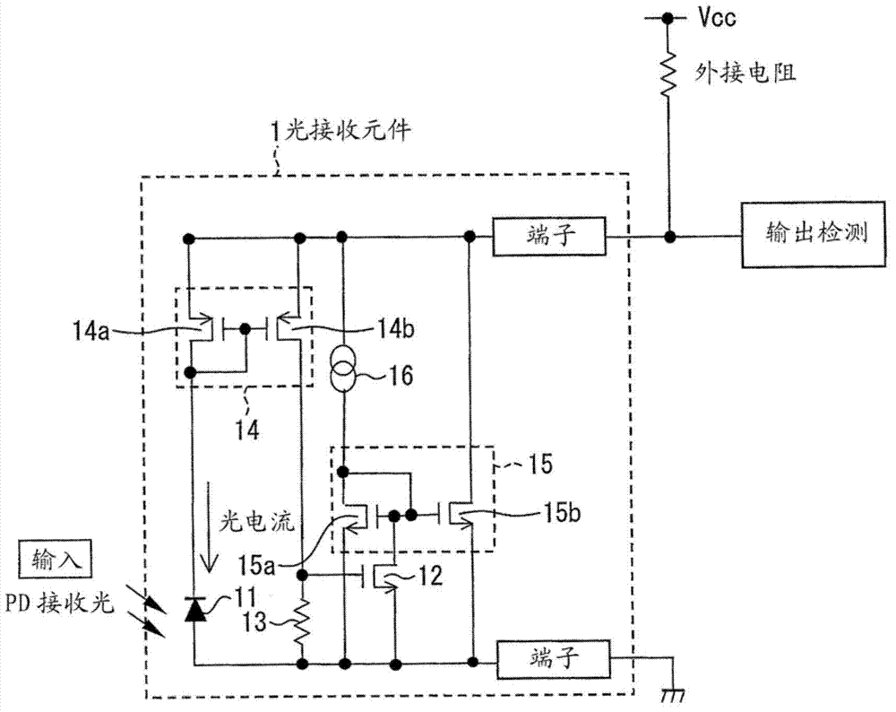
[0084] figure 1 The circuit configuration of the photosensor according to the first embodiment is shown. The light sensor includes a phototransistor represented by an equivalent circuit composed of a photodiode 11 (photoelectric conversion element), a transistor 12 , and a resistor 13 in a light receiving element 1 . The light-receiving element 1 is a two-terminal light-receiving element that outputs a signal by changing the potential of one terminal from the fixed potential of the other terminal by changing the circuit current when light is input. In this embodiment, the terminal at a fixed potential is grounded. Conversely, it is also possible to set the power supply voltage Vcc to a fixed potential. In addition, the light receiving element 1 has a first current mirror circuit 14 composed of transistors 14a a...
Embodiment approach 2
[0094] (Circuit structure of light sensor)
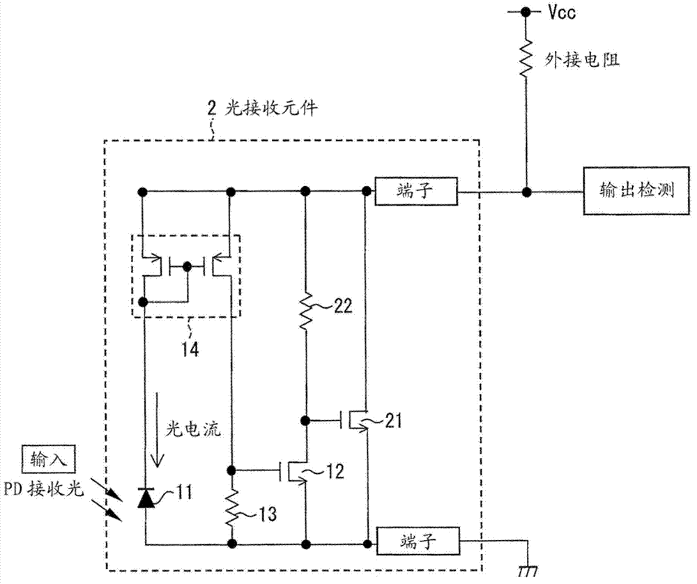
[0095] The optical sensor according to Embodiment 1 has a structure in which photocurrent is amplified by the second current mirror circuit 15 . However, in this structure, especially when the photocurrent is small, the potential fluctuation of the sensor may become insufficient. Therefore, as in the photosensor of Embodiment 2, by converting the photocurrent or the amplified photocurrent to a voltage, and driving the transistor by switching (switching) when reaching a specific voltage, a larger the fixed current. This is advantageous because the electric potential of the sensor can be stably increased.
[0096] refer to figure 2 The circuit configuration of the photosensor according to Embodiment 2 will be described. figure 2 The light sensor shown is in place of the figure 1 The light receiving element 1 is provided with the structure of the light receiving element 2 . and figure 1 The same structure uses the same compon...
Embodiment approach 3
[0103] (Circuit structure of light sensor)
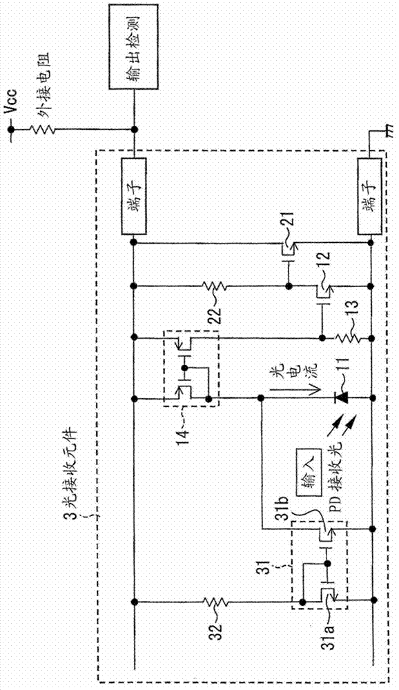
[0104] refer to image 3 The circuit configuration of the photosensor according to Embodiment 3 will be described. image 3 The light sensor shown is in place of the figure 2 The light receiving element 2 is provided with the structure of the light receiving element 3 . and figure 2 The same structure uses the same component number, and the detailed description is omitted.
[0105] The light receiving element 3 includes a current source composed of a third current mirror circuit 31 and a resistor 32 as a current source provided in parallel with the photodiode 11 . Furthermore, an input-side transistor 31 a in the third current mirror circuit 31 is connected to an output detection terminal of the light receiving element 3 via a resistor 32 . The transistor 31 b on the output side of the third current mirror circuit 31 inputs a current to the first current mirror circuit 14 , which is an amplifier common to the photodiode 11 . ...
PUM
 Abstract
Description
Claims
Application Information
 - Generate Ideas
- Intellectual Property
- Life Sciences
- Materials
- Tech Scout
- Unparalleled Data Quality
- Higher Quality Content
- 60% Fewer Hallucinations
Browse by: Latest US Patents, China's latest patents, Technical Efficacy Thesaurus, Application Domain, Technology Topic, Popular Technical Reports.
© 2025 PatSnap. All rights reserved.Legal|Privacy policy|Modern Slavery Act Transparency Statement|Sitemap|About US| Contact US: help@patsnap.com