
Manufacture method of selective emitter crystalline silicon solar cells

A technology of solar cells and emitters, applied in the field of solar cells, can solve the problems of high temperature damage of silicon wafers, high cost, complicated process, etc., and achieve the effects of saving equipment cost, low cost and few process steps.

Inactive Publication Date: 2013-03-20
YINGLI ENERGY CHINA
View PDF7 Cites 2 Cited by
  • Summary
  • Abstract
  • Description
  • Claims
  • Application Information

AI Technical Summary

Problems solved by technology

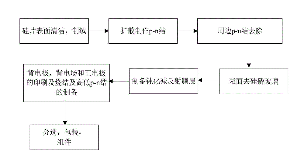
[0004] At present, there are many methods for fabricating selective emitter crystalline silicon solar cell structures. Forming deep and shallow p-n junctions in the process of fabricating selective emitter crystalline silicon solar cells is conducive to improving short-circuit current and open-circuit voltage. The more conventional steps of emitter crystalline silicon solar cells are as follows: figure 1 As shown, diffusion is first performed to form a shallow p-n junction, and then screen-printed phosphorous paste and high-temperature diffusion are performed to form a deep-shallow p-n junction, which increases the cost; in addition, this manufacturing method also includes screen-printed phosphorous paste and high-temperature Diffusion step, high temperature diffusion is easy to cause high temperature damage to silicon wafers, thereby reducing battery efficiency
In addition, the current process is cumbersome, and because the raw materials in the solar cell industry are relatively expensive, the cost is high, and it is not suitable for industrial production.

Method used


Image

  • Manufacture method of selective emitter crystalline silicon solar cells
  • Manufacture method of selective emitter crystalline silicon solar cells
  • Manufacture method of selective emitter crystalline silicon solar cells

Examples


Embodiment 1

[0032]The surface of the silicon wafer is cleaned and textured, and a p-n junction with a diffusion square resistance of 110ohm / sq is produced by controlling the diffusion temperature, gas flow rate and process time of the diffusion furnace. The p-n junction with a diffusion resistance of 110ohm / sq is subjected to steps such as plasma edge etching, surface removal of silicon-phosphorus glass, preparation of an anti-reflection layer, and then printing the positive electrode, the back electrode, and the back electric field. When printing the back electrode, use silver paste with a silver solid content of 70% and a phosphorus content of 2% for printing, and then sinter at 750°C, so that the P atoms on the silicon wafer where the positive electrode is printed are further diffused, and the diffusion resistance It is 55ohm / sq, and the diffusion resistance is 110ohm / sq on the part where the positive electrode is not printed, so that a deep and shallow p-n junction is obtained.


PUM


Abstract

The invention discloses a manufacture method of selective emitter crystalline silicon solar cells. The manufacture method comprises the following steps: cleaning the surface of a silicon wafer, making wool, diffusedly manufacturing shallow p-n knots, manufacturing antireflective film layers, printing a positive electrode and a back electrode, and performing sintering, wherein the step of printing the positive electrode adopts silver slurry containing phosphate to print. As the silver slurry containing phosphate is adopted to print the positive electrode, the silver slurry containing phosphate is subjected to oven-drying, sintering and annealing processes of a sintering furnace after the silver slurry containing phosphate is printed, and phosphorus atoms in the silver slurry are further subjected to phosphorus diffusion when the phosphorus atoms is sintered and annealed to form the positive electrode; a deep diffusion zone is formed in the area of the positive electrode contacted with the silicon wafer, namely deep p-n knobs are formed under the positive electrode; and a shallow diffusion zone is formed in the silicon wafer area not contacted with the positive electrode, so that the deep and the shallow p-n knobs are obtained while the positive electrode is formed. The manufacture method has fewer steps and low cost, and is suitable for industrial production; and as the printing process does not need to use a high-precision printing system, the equipment cost is greatly saved.

Description

technical field [0001] The invention relates to the technical field of solar cells, in particular to a method for manufacturing a selective emitter crystalline silicon solar cell. Background technique [0002] As a clean and environmentally friendly new energy source, the application of solar cells is becoming more and more popular. However, due to the high cost of this battery, its rapid popularization is limited. In order to reduce the production cost and improve the conversion efficiency of solar cells, new technologies need to be continuously developed. Among them, the manufacturing process of selective emitter cells has become a new process for improving the efficiency of solar cells due to its simplicity and effectiveness. [0003] Selective emitter (SE-Selective Emiter) crystalline silicon solar cells, that is, heavy doping is carried out at the contact part between the metal grid line (electrode) and the silicon wafer, and light doping is carried out at the part bet...

Claims


Application Information

Patent Timeline
Patent Type & Authority Applications(China)
IPC IPC(8): H01L31/18
CPCY02P70/50
Inventor 马红娜杨伟光王海亮张红妹
Owner YINGLI ENERGY CHINA
Learn More