Al technical title is built by PatSnap Al team. It summarizes the technical point description of the patent document.
An ESD protection, three-path technology, used in semiconductor devices, electrical solid state devices, circuits, etc., can solve the problems of increasing the design difficulty of high-voltage ESD protection devices, narrowing the ESD design window, and easily entering the latch state, etc. High-voltage ESD protection, small on-resistance, and the effect of increasing the discharge path
Active Publication Date: 2015-02-25
铜陵汇泽科技信息咨询有限公司
View PDF5 Cites 0 Cited by
Summary
Abstract
Description
Claims
Application Information
AI Technical Summary
This helps you quickly interpret patents by identifying the three key elements:
Problems solved by technology
Method used
Benefits of technology
Problems solved by technology
This is because in order to obtain a reliable and practical high-voltage ESD protection device, it is necessary to consider the high operating voltage in the circuit and not to cause breakdown of the gate oxide of the MOS device in the circuit. Therefore, it is necessary to accurately design a high-performance ESD high-voltage device. Both a high sustain voltage and a low trigger voltage between the operating voltage and the breakdown voltage of the gate oxide are required. The above factors narrow the available ESD design window and increase the difficulty of designing high-voltage ESD protection devices.
[0003]The above-mentioned on-chip IC low-voltage ESD protection devices are easy to enter the latch-up state due to the high operating voltage of the high-voltage circuit. Most of the devices are no longer suitable for high-voltage ESD protection, and now There are high-voltage ESD protection devices such as common LDMOS, whose breakdown voltage is not determined by the source-drain implantation conditions, but mainly depends on the ion implantation in the drift region
If the distribution of implanted impurities in the drift region of the LDMOS device is optimized only, it will increase the surface electric field of the drift region during triggering, making the gate oxide more susceptible to damage
Method used
Image
Click on the blue label to locate the original text in one second.
Reading with bidirectional positioning of images and text.
Examples
Embodiment Construction
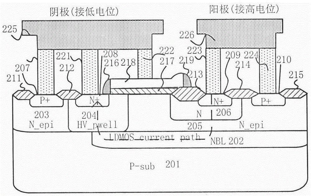
[0027] The present invention proposes a bidirectional three-path high-voltage ESD protection device combining SCR and NLDMOS, because its trigger voltage is mainly affected by the impurity concentration of the heavily doped N-type buried layer, and it has a longer current conduction path, so the energy efficiency reduces the trigger voltage of the device, increases the maintenance voltage and the secondary breakdown current, and at the same time has the function of bidirectional ESD protection, and also has the advantages of small leakage current, small on-resistance, and fast response speed.
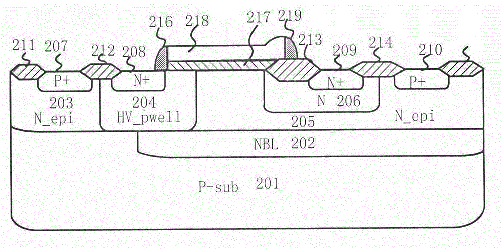
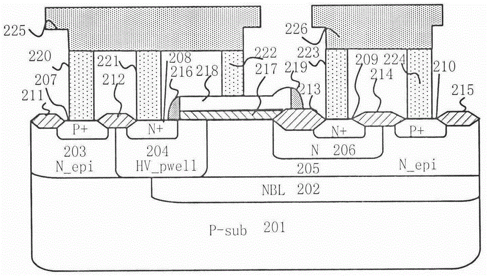
[0028] like figure 1 As shown, it is a structural cross-sectional view of an example device of the present invention, specifically a high-voltage ESD protection device with bidirectional and three-path conduction combined with SCR and NLDMOS, including a P-substrate 201, an N+ buried layer 202, a first N-type epitaxial 203, the second N-type epitaxy 205, the high-voltage P well 204, the...
PUM
Abstract
The invention provides a bidirectional tri-path turn-on high-voltage ESD (Electro-Static Discharge) protective device which can be used in an on-chip IC (Integrated Circuit) high-voltage ESD protective circuit. The bidirectional tri-path turn-on high-voltage ESD protective device comprises a P minus substrate, an N plus buried layer, a left N-type epitaxy, a right N-type epitaxy, a drifting area, a high-voltage P trap, a drain region, a source region, a polysilicon gate, a positive pole contact area and a negative pole contact area, wherein the drifting area, the high-voltage P trap, the drain region, the source region and the polysilicon gate form an NLDMOS (laterally diffused metal oxide semiconductor) structure, and the positive pole contact area, the N plus buried layer, the high-voltage P trap and the source region form a positive SCR (semiconductor control rectifier)structure, so that two high-voltage ESD current discharge paths are formed to improve secondary striking current of the device and reduce the turn-on resistance and trigger voltage; and the negative pole contact area, the left N-type epitaxy, the high-voltage P trap, the N plus buried layer and the drain region form a reverse SCR structure to form a reverse high-voltage ESD current discharge path. The current paths of the two SCR structures are longer, so that the maintaining voltage of the device can be improved, bidirectional discharge of ESD current can be realized, and the device has bidirectional ESD protection function.
Description
technical field [0001] The invention belongs to the field of electrostatic protection of integrated circuits and relates to a high-voltage ESD protection device, in particular to a high-voltage ESD protection device with bidirectional and three-path conduction, which can be used to improve the reliability of on-chip IC high-voltage ESD protection. Background technique [0002] ESD, which refers to a physical phenomenon of electrostatic charge transfer between objects at different potentials, has attracted increasing attention as a phenomenon that causes product failure in ICs. At present, the low-voltage electrostatic discharge protection for submicron, deep submicron and nanometer-scale ICs has been extensively and in-depth researched, and there are various low-voltage ESD protection devices such as diodes, triodes, thyristors (SCR) and Devices such as gate-grounded NMOS have been reported in related literature at home and abroad. From the experimental data in the research...
Claims
Application Information
Patent Timeline
Application Date:The date an application was filed.
Publication Date:The date a patent or application was officially published.
First Publication Date:The earliest publication date of a patent with the same application number.
Issue Date:Publication date of the patent grant document.
PCT Entry Date:The Entry date of PCT National Phase.
Estimated Expiry Date:The statutory expiry date of a patent right according to the Patent Law, and it is the longest term of protection that the patent right can achieve without the termination of the patent right due to other reasons(Term extension factor has been taken into account ).
Invalid Date:Actual expiry date is based on effective date or publication date of legal transaction data of invalid patent.