
Method for improving uniformity of axial resistivity of czochralski silicon and obtained monocrystalline silicon

A technology of resistivity and uniformity, which is applied in the field of semiconductor materials, can solve the problems of small equilibrium segregation coefficient and poor axial resistivity uniformity of antimony-doped Czochralski single crystal silicon, and achieve the goal of improving uniformity and good industrial application prospects Effect

Active Publication Date: 2013-02-06
ZHEJIANG UNIV
View PDF2 Cites 24 Cited by
  • Summary
  • Abstract
  • Description
  • Claims
  • Application Information

AI Technical Summary

Problems solved by technology

[0008] However, similar to gallium-doped single crystal silicon, the equilibrium segregation coefficient of antimony in silicon is also very small (about 0.023), which also leads to poor axial resistivity uniformity of antimony-doped Czochralski single crystal silicon.

Method used


Image

  • Method for improving uniformity of axial resistivity of czochralski silicon and obtained monocrystalline silicon
  • Method for improving uniformity of axial resistivity of czochralski silicon and obtained monocrystalline silicon
  • Method for improving uniformity of axial resistivity of czochralski silicon and obtained monocrystalline silicon

Examples


Embodiment 1

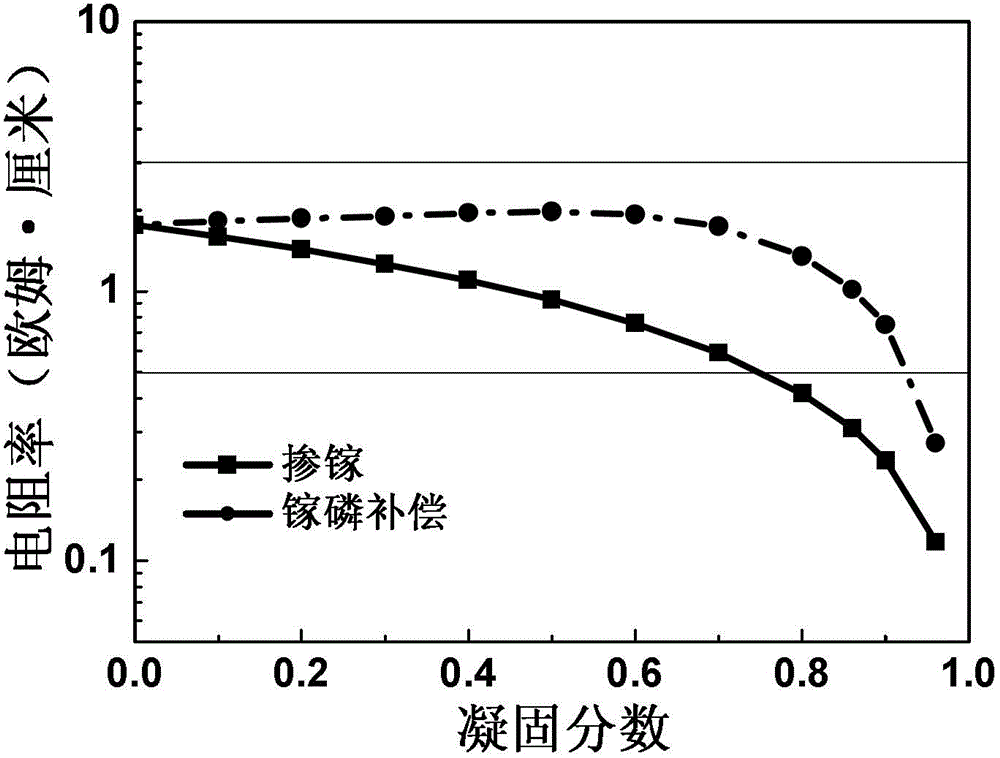
[0065] Add 60kg of high-purity polysilicon raw material into the quartz crucible, and at the same time add 2.982g of high-purity gallium (the target resistivity of the control head is 1.8 ohm.cm).

[0066] Under the protection of argon, the temperature is gradually raised to above 1420°C to completely melt the high-purity polysilicon. According to the conventional crystal growth parameters, the seeding and shouldering are carried out to enter the equal-diameter growth stage, and the crystal pulling rate is controlled to 1.2 mm / min, and the crystal diameter is 150 mm.

[0067] The furnace pressure is controlled to 20 Torr, and the argon gas flow rate is 70 slpm (standard liter per minute).

[0068] Set the parameters for the dopant gas:

[0069] 1) Phosphine diluted with argon is used as the doping gas, and the volume ratio of phosphine to argon is 1:1000;

[0070] 2) Assuming that the doping efficiency is 100% (the impurities introduced by the doping gas can all enter into t...

Embodiment 2

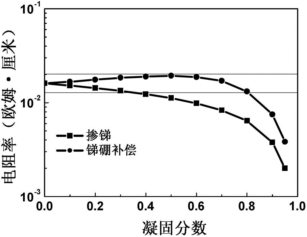
[0075] Add 60 kg of high-purity polysilicon raw material into the quartz crucible, and at the same time add 416.64 g of high-purity antimony (the target resistivity of the control head is 0.016 ohm.cm).

[0076] Under the protection of argon, the temperature is gradually raised to above 1420°C to completely melt the polysilicon. According to the conventional crystal growth parameters, the seeding and shouldering are carried out to enter the equal-diameter growth stage, the crystal pulling rate is controlled to 0.8mm / min, and the crystal diameter is 150mm.

[0077] The furnace pressure is controlled to 20 Torr, and the argon gas flow rate is 70 slpm.

[0078] Set the parameters for the dopant gas:

[0079] 1) Diborane diluted with argon, the volume ratio of diborane to argon is 1:100;

[0080] 2) Assuming that the doping efficiency is 100%, the flow rate of the doping gas is set to 97.58 sccm.

[0081] After the equal-diameter growth is completed, the dopant gas is turned of...


PUM


Abstract

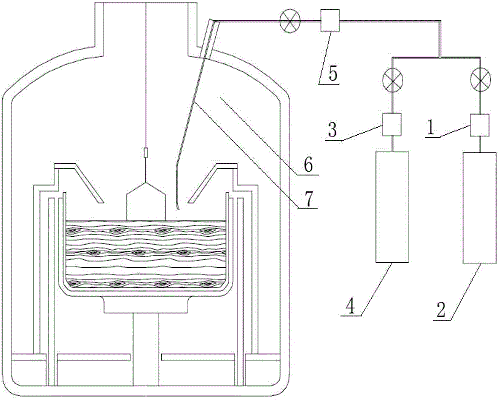
The invention discloses a method for improving the uniformity of axial resistivity of czochralski silicon. The method comprises the steps as follows: (1) melting a polycrystalline silicon raw material and a solid doping agent in an argon atmosphere to obtain stable molten silicon; (2) introducing seed crystals into the stable molten silicon, and conducting constant diameter growth on the crystals after necking and shouldering processes; and (3) during the constant diameter growth period, adding dopant gas with the conductive type opposite to that of the solid doping agent until the growth of the czochralski silicon is fulfilled. According to the method, the type and the usage amount of the dopant gas are convenient to control, various required impurity concentration distributions can be obtained, the utilization rate of the czochralski silicon is increased, and the uniformity of the resistivity of the czochralski silicon is remarkably improved.

Description

technical field [0001] The invention relates to the field of semiconductor materials, in particular to a method for improving the axial resistivity uniformity of Czochralski single crystal silicon through a gas phase doping method and the obtained single crystal silicon. Background technique [0002] In the foreseeable future, photovoltaic power generation is the most important renewable energy technology. According to the forecast of the European Photovoltaic Industry Association (EPIA), photovoltaic power generation will meet nearly 10% of the world's electricity demand in 2030. [0003] Current solar cells are mainly manufactured based on boron-doped single crystal silicon materials, but because single crystal silicon contains boron and oxygen at the same time, boron-oxygen complexes will be formed during use, resulting in lower photoelectric conversion efficiency of solar cells. With a drop of more than 10%, the performance of the solar cell is significantly reduced. T...

Claims


Application Information

Patent Timeline
IPC IPC(8): C30B15/00C30B15/04C30B29/06
Inventor 杨德仁陈鹏余学功吴轶超陈仙子
Owner ZHEJIANG UNIV
Learn More