Method for forming SOI MOSFET (Silicon On Insulator Metal-Oxide-Semiconductor Field Effect Transistor) body contact by using side wall process

A body contact and process technology, applied in the field of forming electronic components, can solve the problems of destroying the isolation effect of SOIMOSFET devices, complicating the device manufacturing process, reducing production costs, etc., to achieve anti-floating body effect, prevent self-heating effect, increase Effectiveness

Inactive Publication Date: 2015-07-22
HARBIN ENG UNIV
View PDF3 Cites 0 Cited by
  • Summary
  • Abstract
  • Description
  • Claims
  • Application Information

AI Technical Summary

Problems solved by technology

Although this method can suppress the floating body effect of SOI MOSFET devices, it sometimes destroys the isolation effect of SOI MOSFET devices. At the same time, since contact trenches are to be formed, mask plates and etching techniques must be used repeatedly in the formation method. Complicates the manufacturing process of the device, which is not conducive to reducing production costs

Method used


Image

  • Method for forming SOI MOSFET (Silicon On Insulator Metal-Oxide-Semiconductor Field Effect Transistor) body contact by using side wall process
  • Method for forming SOI MOSFET (Silicon On Insulator Metal-Oxide-Semiconductor Field Effect Transistor) body contact by using side wall process
  • Method for forming SOI MOSFET (Silicon On Insulator Metal-Oxide-Semiconductor Field Effect Transistor) body contact by using side wall process

Examples


Embodiment Construction

[0033] The present invention is described in detail below in conjunction with accompanying drawing example:

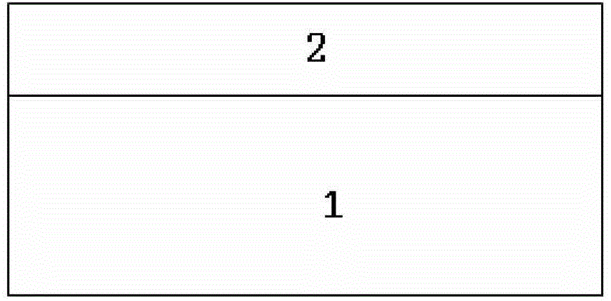
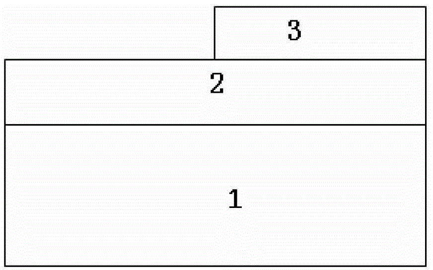
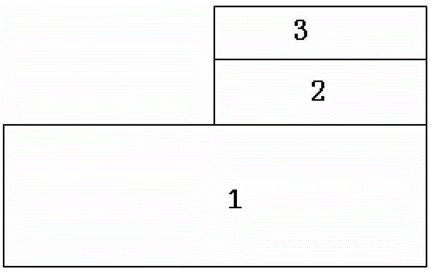
[0034] combine figure 1 . A masking film 2 is shown deposited on an underlying semiconductor substrate 1 . The material of the underlying semiconductor substrate 1 can be freely selected, for example: silicon, germanium, group III~V compound semiconductor materials, group II~VI compound semiconductor materials or other compound semiconductor materials, etc., and single crystal materials can also be used. For single crystal materials It can also be made into an n-type substrate or a p-type substrate by doping. The material used for the masking film 2 can be such as SiO 2 The same hard masking material can also be applied with a soft masking material like photoresist, but no matter which type of masking material is used, it should be noted that the material used for the masking film cannot be the same as the underlying semiconductor substrate material to prevent etchi...


PUM


Abstract

The invention provides a method for forming an SOI MOSFET (Silicon On Insulator Metal-Oxide-Semiconductor Field Effect Transistor) body contact by using a side wall process. The SOI MOSFET body contact comprises a bottom semiconductor substrate 1 formed through etching, a left buried implanted oxide layer 6(A) and a right buried implanted oxide layer 6(B) on the bottom semiconductor substrate (1), a top silicon film (7), a grid oxide layer (8) growing on the top silicon film (7), and a polycrystalline silicon gate (9) positioned on the grid oxide layer (8). The SOI MOSFET body contact is characterized in that a leading-out terminal of the body contact (1) is positioned between horizontal planes of two bottom semiconductor substrates (1) positioned in different heights. The SOI MOSFET body contact structure can be used for leading excessive holes in a neutral body region out for realizing an anti-floater effect, and can prevent a self-heating effect. The invention method also provides a forming method of the SOI MOSFET body contact, which has the advantages of simplifying manufacture procedures, lowering manufacture cost and improving device reliability.

Description

technical field [0001] The invention relates to an electronic component, and the invention also relates to a method for forming the electronic component. Specifically, it is an SOI MOSFET body contact structure utilizing a sidewall process and a forming method thereof. Background technique [0002] As a full dielectric isolation technology, SOI technology has many incomparable advantages over bulk silicon technology. However, SOI devices also have some parasitic effects, among which the floating body effect of partially depleted SOI devices is the biggest problem compared with bulk silicon devices, which has also become one of the reasons restricting the development and wide application of SOI technology. Floating body effect will produce kink effect, drain breakdown voltage reduction, abnormal subthreshold slope, etc., which seriously affect the performance of the device. [0003] Due to the impact of the floating body effect on device performance, how to suppress the flo...

Claims


Application Information

Patent Timeline
Patent Type & Authority Patents(China)
IPC IPC(8): H01L29/78H01L29/06H01L21/336
Inventor 王颖包梦恬曹菲胡海帆
Owner HARBIN ENG UNIV
Why Eureka
Try Eureka