A method for forming body contact of soi MOSFET using sacrificial layer

A body contact and sacrificial layer technology, applied in semiconductor/solid-state device manufacturing, electrical components, circuits, etc., can solve the problems of destroying the isolation effect of SOIMOSFET devices, complicating the device manufacturing process, and cumbersome manufacturing steps.

Inactive Publication Date: 2015-09-30
HARBIN ENG UNIV
View PDF3 Cites 0 Cited by
  • Summary
  • Abstract
  • Description
  • Claims
  • Application Information

AI Technical Summary

Problems solved by technology

Although this method can suppress the floating body effect of SOI MOSFET devices, it sometimes destroys the isolation effect of SOI MOSFET devices. The manufacturing process of the device is complicated, and the manufacturing steps are cumbersome, which is not conducive to reducing the production cost

Method used


Image

  • A method for forming body contact of soi MOSFET using sacrificial layer
  • A method for forming body contact of soi MOSFET using sacrificial layer
  • A method for forming body contact of soi MOSFET using sacrificial layer

Examples


Embodiment Construction

[0027] The present invention is described in detail below in conjunction with accompanying drawing example:

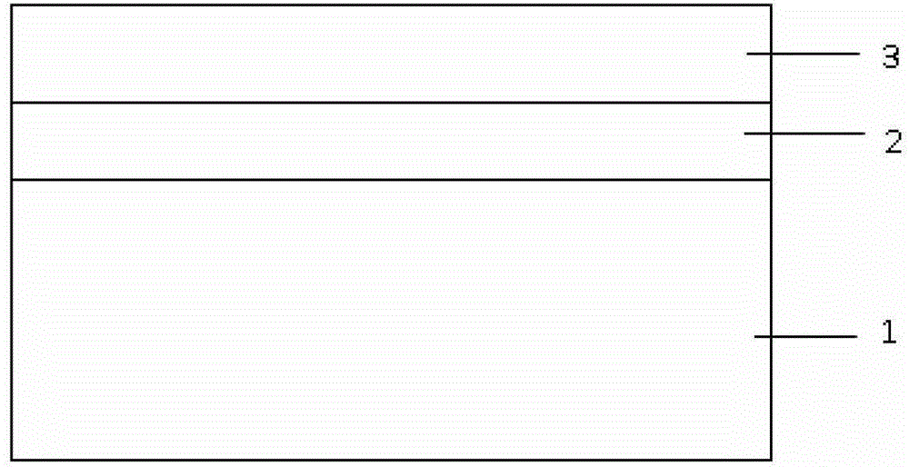
[0028] combine figure 1 . Buried SiO is deposited on the underlying semiconductor substrate 1 as shown 2 Layer 2, in buried SiO 2 A SiGe masking film 3 is deposited on layer 2 . The material of the underlying semiconductor substrate 1 can be freely selected, for example: silicon, germanium, group III~V compound semiconductor materials, group II~VI compound semiconductor materials or other compound semiconductor materials, etc., and single crystal materials can also be used. Can be doped to make it an n-type substrate or a p-type substrate.

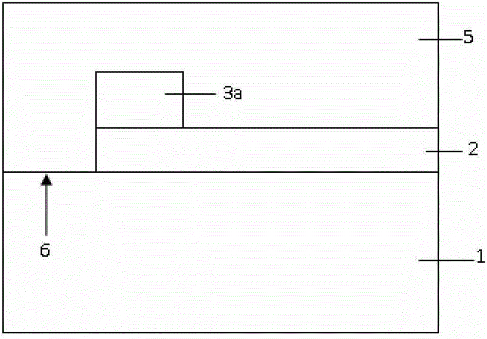
[0029] combine figure 2 . Coat photoresist 4 on SiGe masking film 3, make photoresist 4 cover the small area of ​​SiGe masking film 3, etch and remove uncoated SiGe masking film 3 until the buried SiO is exposed 2 layer 2, and make the buried SiO on both sides of the remaining SiGe masking film 3a 2 Layer 2 has different a...


PUM


Abstract

The invention provides a body contact forming method by utilizing an SOI (silicon on insulator) MOSFET (metal oxide semiconductor field effect transistor) of a sacrificial layer. The method comprises the following steps of: depositing a buried SiO2 layer (2) on a semiconductor substrate (1) on a bottom layer, and depositing a SiGe mask membrane (3) on the buried SiO2 layer (2); etching for the first time and exposing the buried SiO2 layer (2); etching for the second time and maintaining the buried layer SiO2 layer (2) with a large area at the right side of the SiGe mask membrane (3); carrying out epitaxial growth of a silicon membrane (5) at the top layer; forming a gate oxide layer (7), and depositing a polycrystalline gate (8); etching for the third time and removing the silicon membrane (5) at the top layer of a glue-free part; etching horizontally for the fourth time and removing the remained SiGe mask membrane (3a); and carrying out epitaxial growth and compensating the silicon membrane at the top layer (5), pouring P+ ions, and depositing a metal electrode. The body contact forming method by utilizing the SOI MOSFET of the sacrificial layer has the advantages of reducing the use of the mask membrane plate, simplifying the manufacturing technology flow, and lowering the manufacturing cost.

Description

technical field [0001] The invention relates to a method for forming electronic components. Specifically, it is a method for forming SOI MOSFET body contact using a sacrificial layer. Background technique [0002] As a full dielectric isolation technology, SOI technology has many incomparable advantages over bulk silicon technology. However, SOI devices also have some parasitic effects, among which the floating body effect of partially depleted SOI devices is the biggest problem compared with bulk silicon devices, which has also become one of the reasons restricting the development and wide application of SOI technology. Floating body effect will produce kink effect, drain breakdown voltage reduction, abnormal subthreshold slope, etc., which seriously affect the performance of the device. [0003] Due to the impact of the floating body effect on device performance, how to suppress the floating body effect has become a hot spot in the research of SOI devices. The suppressi...

Claims


Application Information

Patent Timeline
Patent Type & Authority Patents(China)
IPC IPC(8): H01L21/336
Inventor 王颖包梦恬曹菲邵雷
Owner HARBIN ENG UNIV
Why Eureka
Try Eureka