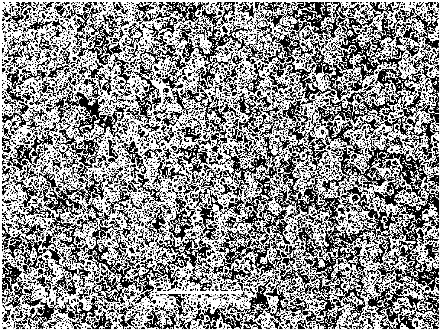
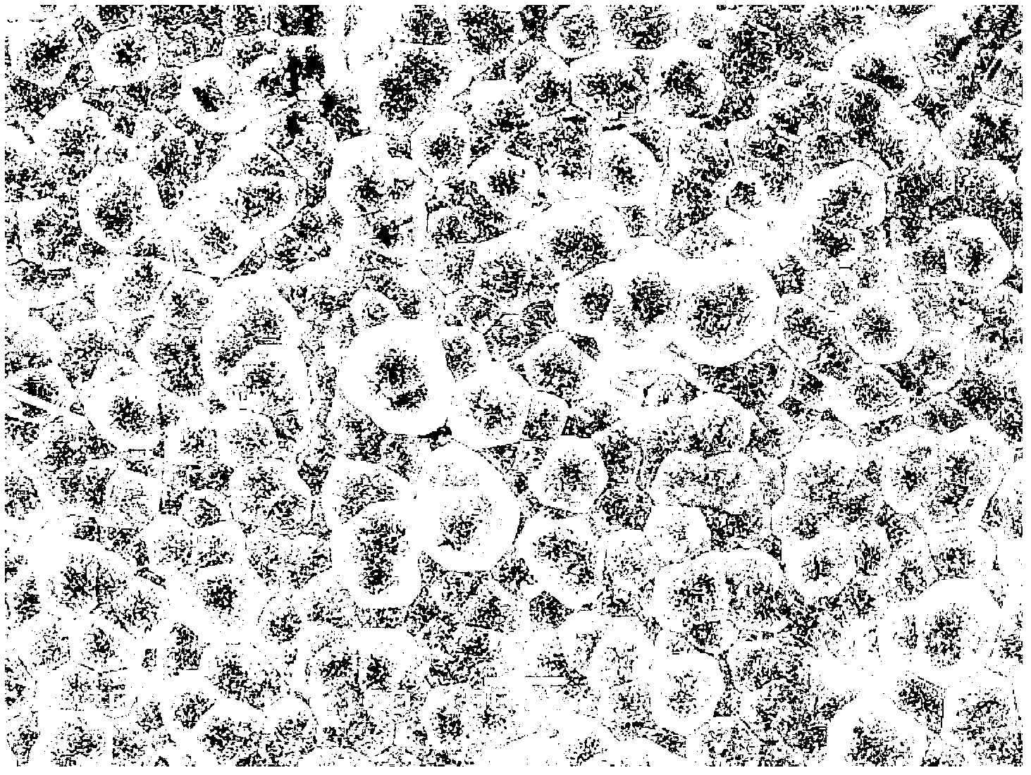
Method for preparing silicon carbide coating on graphite surface
A silicon carbide coating and graphite technology, applied in the field of high-performance graphite coating, can solve the problems of short service life, cracking and coating failure of silicon carbide coated graphite, avoiding thermal mismatch, firm bonding and no cracking Effect
- Summary
- Abstract
- Description
- Claims
- Application Information
AI Technical Summary
Problems solved by technology
Method used
Image
Examples
Embodiment 1
[0019] Step 1. Place the graphite crucible with solid silicon material in a high-temperature graphitization furnace, place the graphite substrate on the graphite support in the graphite crucible, and keep it warm for 1 hour at a temperature of 1500°C and a vacuum of 100Pa. Silicon vapor reacts directly with the carbon on the surface of the graphite substrate to form a layer of silicon carbide coating (CVR silicon carbide coating); the amount of the solid silicon material is measured by the external area of the graphite substrate, and the external area of the graphite substrate per square centimeter is measured by the solid silicon material 5g;
[0020] Step 2. Place the graphite substrate with a silicon carbide coating on the surface in step 1 in a chemical vapor deposition furnace, and feed hydrogen and dilution gas into the furnace at a temperature of 1000 ° C, and use the bubbling gasification method Pass trichloromethylsilane into the furnace after being vaporized, kee...
Embodiment 2
[0024] Step 1. Place the graphite crucible containing solid silicon material in a high-temperature graphitization furnace, place the graphite substrate on the graphite support in the graphite crucible, and keep it warm for 5 hours at a temperature of 1500 ° C and a vacuum of 100 Pa. Use Silicon vapor reacts directly with the carbon on the surface of the graphite substrate to form a layer of silicon carbide coating (CVR silicon carbide coating); the amount of the solid silicon material is measured by the external area of the graphite substrate, and the external area of the graphite substrate per square centimeter is measured by the solid silicon material 20g;
[0025] Step 2. Place the graphite substrate with a silicon carbide coating on the surface in step 1 in a chemical vapor deposition furnace, and feed hydrogen and dilution gas into the furnace at a temperature of 1000 ° C, and use the bubbling gasification method Pass trichloromethylsilane into the furnace after being...
Embodiment 3
[0028] Step 1. Place the graphite crucible with solid silicon material in a high-temperature graphitization furnace, place the graphite substrate on the graphite support in the graphite crucible, and keep it warm for 1 hour at a temperature of 1650°C and a vacuum of 500Pa. Use Silicon vapor reacts directly with the carbon on the surface of the graphite substrate to form a layer of silicon carbide coating (CVR silicon carbide coating); the amount of the solid silicon material is measured by the external area of the graphite substrate, and the external area of the graphite substrate per square centimeter is measured by the solid silicon material 10g;
[0029] Step 2. Place the graphite substrate with a silicon carbide coating on the surface in step 1 in a chemical vapor deposition furnace, and feed hydrogen and dilution gas into the furnace at a temperature of 1100 ° C, and use the bubbling gasification method After trichloromethylsilane is gasified, it is passed into the fu...
PUM
 Abstract
Description
Claims
Application Information
 - R&D
- Intellectual Property
- Life Sciences
- Materials
- Tech Scout
- Unparalleled Data Quality
- Higher Quality Content
- 60% Fewer Hallucinations
Browse by: Latest US Patents, China's latest patents, Technical Efficacy Thesaurus, Application Domain, Technology Topic, Popular Technical Reports.
© 2025 PatSnap. All rights reserved.Legal|Privacy policy|Modern Slavery Act Transparency Statement|Sitemap|About US| Contact US: help@patsnap.com


