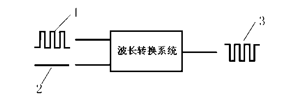
All-optical wavelength conversion integrated chip based on transient chirp jump
An all-optical wavelength conversion and integrated chip technology, applied in the fields of optics, nonlinear optics, instruments, etc., can solve the problems of difficult integration, inability to achieve integration, miniaturization and productization, and bulky wavelength conversion devices. effect of integration, overcoming electron rate bottlenecks, improving gain effective recovery time
- Summary
- Abstract
- Description
- Claims
- Application Information
AI Technical Summary
Problems solved by technology
Method used
Image

Examples
Embodiment
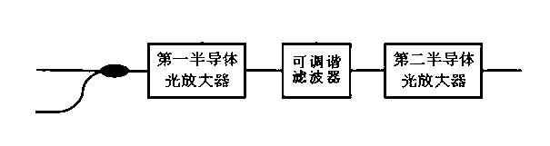
[0022] Under the following specific parameters, the simulation of the all-optical wavelength conversion chip based on the transient chirp transition provided by the present invention is carried out. The semiconductor optical amplifier has an active region length of 1 mm, a carrier lifetime of 60 ps, an operating current of 400 mA, and a mode loss of 17 cm -1 , the TE mode confinement factor is 0.2, and the TM mode confinement factor is 0.14; the pump light has a wavelength λ pump Gaussian pulsed light with a working rate of 1550nm, a working rate of 160Gb / s, a pulse width of 2ps, and a pulse peak power of 20mW; the probe light is a wavelength λ probe DC light at 1565nm with an average power of 1mW. The working band of the arrayed waveguide grating is 1550nm, the passband spacing is 200GHz, and the sideband suppression ratio is 20dB. The delay time of the delay interferometer is 2ps. The specific implementation above realizes the transfer of the digital signal from the ...
PUM
| Property | Measurement | Unit |
|---|---|---|
| length | aaaaa | aaaaa |
| charge carrier lifetime | aaaaa | aaaaa |
Abstract
Description
Claims
Application Information
 - R&D
- Intellectual Property
- Life Sciences
- Materials
- Tech Scout
- Unparalleled Data Quality
- Higher Quality Content
- 60% Fewer Hallucinations
Browse by: Latest US Patents, China's latest patents, Technical Efficacy Thesaurus, Application Domain, Technology Topic, Popular Technical Reports.
© 2025 PatSnap. All rights reserved.Legal|Privacy policy|Modern Slavery Act Transparency Statement|Sitemap|About US| Contact US: help@patsnap.com