Zn-doped Ge2Sb2Te5 phase-change storage film material and preparation method thereof
A phase-change storage and thin-film material technology, which is applied in metal material coating process, ion implantation plating, coating, etc., can solve the problems that affect the reliability of devices that affect the erasing and writing speed, short data storage life, and poor crystallization speed, etc. , achieve good thermal stability and data retention, improve crystallization activation energy, and improve data retention life
- Summary
- Abstract
- Description
- Claims
- Application Information
AI Technical Summary
Problems solved by technology
Method used
Image
Examples
Embodiment 1
[0023] A kind of Zn doped Ge of the present invention2 Sb 2 Te 5 Phase change memory thin film material, its chemical structure is Zn X (Ge 2 Sb 2 Te 5 ) 100-X , where 0<x<20, the specific preparation process is as follows:
[0024] 1. In the magnetron sputtering coating system (JGP-450 type), the alloy zinc target is installed in the magnetron direct current (DC) sputtering target, and the Ge 2 Sb 2 Te 5 The target is installed in the magnetron radio frequency (RF) sputtering target, and the quartz sheet or silicon oxide sheet is used as the substrate. The sputtering chamber of the magnetron sputtering coating system is vacuumed until the vacuum degree of the chamber reaches 1.6×10 -4 Pa, and then pass high-purity argon gas with a volume flow rate of 47.6ml / min (SCCM standard condition milliliter per minute) into the sputtering chamber until the pressure in the sputtering chamber reaches the ignition pressure of 0.3Pa required for sputtering, and then control the all...
Embodiment 2
[0028] Basically the same as Example 1, the difference is that in the sputtering process, the sputtering power of the alloy Zn target is controlled to be 3W, and the alloy Ge 2 Sb 2 Te 5 The sputtering power of the target is 100W, and the obtained Zn-doped Ge 2 Sb 2 Te 5 Zn phase change memory film X (Ge 2 Sb 2 Te 5 ) 100-X The Zn content (at%) is 6.37%.
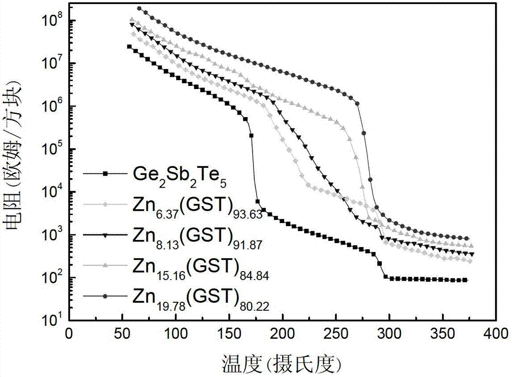
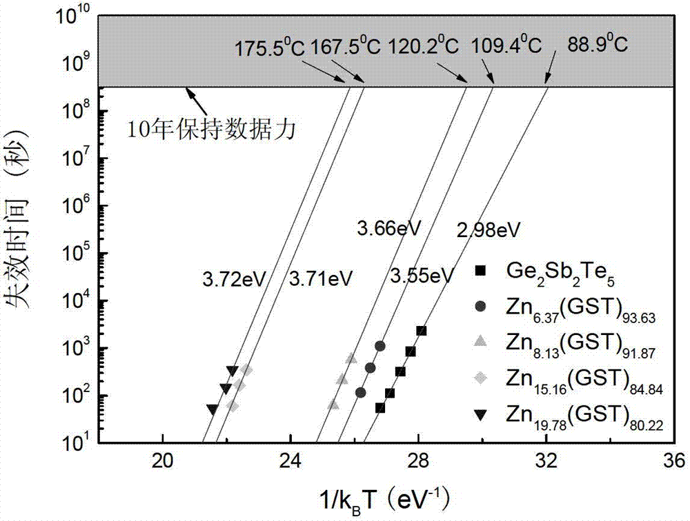
[0029] The prepared film was tested for in-situ resistance performance, and the test results were as follows: figure 1 with figure 2 shown, from figure 1 with figure 2 It can be seen that the performance index of the thin film prepared in embodiment 2 is as follows; crystallization temperature T c is 188°C, the crystallization activation energy ( E a ) is 3.55eV, and the maximum temperature for data storage for 10 years is 109.4°C.
Embodiment 3
[0031] Basically the same as Example 1, the difference is that in the sputtering process, the sputtering power of the alloy Zn target is controlled to be 3W, and the alloy Ge 2 Sb 2 Te 5 The sputtering power of the target was 75W, the sputtering time was 200 seconds, and the Zn content (at%) in the prepared film components was 8.13%.
[0032] The prepared film was tested for in-situ resistance performance, and the test results were as follows: figure 1 with figure 2 shown, from figure 1 with figure 2 It can be seen that the performance index of the thin film prepared in Example 3 is as follows: crystallization temperature ( T c ) is 196℃, and the crystallization activation energy ( E a ) is 3.66eV, and the maximum temperature for data storage for 10 years is 120.2°C.
PUM
| Property | Measurement | Unit |
|---|---|---|
| Crystallization temperature | aaaaa | aaaaa |
| Crystallization temperature | aaaaa | aaaaa |
| Crystallization temperature | aaaaa | aaaaa |
Abstract
Description
Claims
Application Information
 - R&D Engineer
- R&D Manager
- IP Professional
- Industry Leading Data Capabilities
- Powerful AI technology
- Patent DNA Extraction
Browse by: Latest US Patents, China's latest patents, Technical Efficacy Thesaurus, Application Domain, Technology Topic, Popular Technical Reports.
© 2024 PatSnap. All rights reserved.Legal|Privacy policy|Modern Slavery Act Transparency Statement|Sitemap|About US| Contact US: help@patsnap.com


