Method for copper dual damascene structure having ultralow dielectric constant layer
A technology of ultra-low dielectric constant and dielectric constant, applied in the field of microelectronics
- Summary
- Abstract
- Description
- Claims
- Application Information
AI Technical Summary
Problems solved by technology
Method used
Image
Examples
Embodiment Construction
[0031] The present invention will be further described below in conjunction with the principle diagram and specific operation examples.
[0032] A method of copper double damascene structure with ultra-low dielectric constant layer, which includes the following steps:
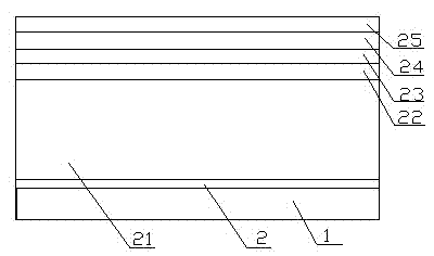
[0033] As shown in FIG. 2A, step S1: providing a substrate 1, which is a substrate with a semiconductor structure;
[0034] Step S2: deposit an etching stop layer 2 and a first interlayer dielectric layer 21 on the substrate 1 from bottom to top, the first interlayer dielectric layer 21 being a low dielectric constant layer;
[0035] Wherein, in this step, the etching stop layer 2 fabricated on the substrate 1 is an etching stop layer containing nitrogen elements, for example, it can be a silicon nitride layer or a carbon-doped silicon nitride material. .
[0036] In addition, the first interlayer dielectric layer 21 is made of a low dielectric constant material with a dielectric constant between 4 and 2.5, for example,...
PUM
 Abstract
Description
Claims
Application Information
 - R&D
- Intellectual Property
- Life Sciences
- Materials
- Tech Scout
- Unparalleled Data Quality
- Higher Quality Content
- 60% Fewer Hallucinations
Browse by: Latest US Patents, China's latest patents, Technical Efficacy Thesaurus, Application Domain, Technology Topic, Popular Technical Reports.
© 2025 PatSnap. All rights reserved.Legal|Privacy policy|Modern Slavery Act Transparency Statement|Sitemap|About US| Contact US: help@patsnap.com


