Organic semiconductor materials, their preparation methods and applications
A technology of organic semiconductors and organic palladium, which is applied in semiconductor/solid-state device manufacturing, semiconductor devices, organic chemistry, etc., can solve the problems of blue light-emitting materials such as poor luminous efficiency and stable carrier transport performance, and achieve excellent solubility , Improve the stability of performance, improve the effect of electron transfer rate
- Summary
- Abstract
- Description
- Claims
- Application Information
AI Technical Summary
Problems solved by technology
Method used
Image
Examples
preparation example Construction
[0028] The embodiment of the present invention further provides the method for preparing the above-mentioned organic semiconductor material, including the following steps:
[0029] Step S01, respectively providing boric acid of structural formula I or boric acid ester of structural formula II, and tripolyindene monomer of structural formula III;
[0030] Structural formula I is: Structural formula II is: Structural formula III is:
[0031] Step S02, in an inert atmosphere, dissolve the triindene monomer of the structural formula III and the boric acid of the structural formula I or the boric acid ester of the structural formula II in an organic solvent at a molar ratio of 1:3-4.5, and perform a Suzuki reaction to obtain an organic Semiconductor material precursor, structural formula (IV) is as follows:
[0032]
[0033] Step S03, in an inert atmosphere, at a temperature of -78 to 180°C, dissolve the organic semiconductor material precursor in an organic solvent, and ...
Embodiment 1
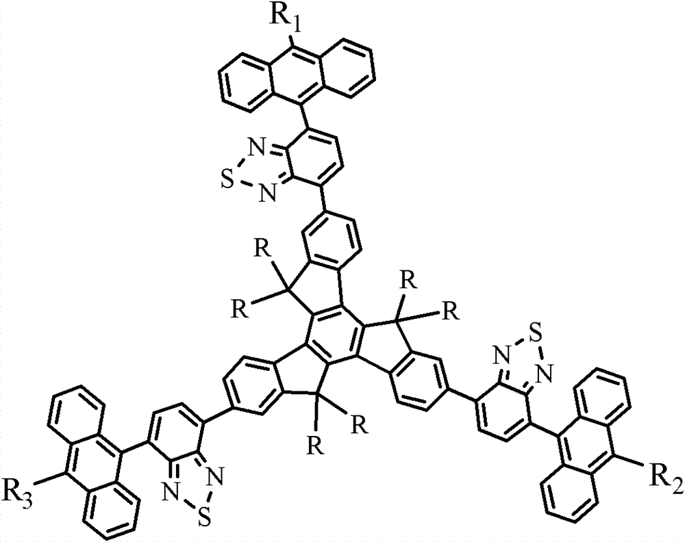
[0074] Example of the present invention 2-(5-(10-cyano-anthracene-9-yl)benzothiadiazol-2-yl)-7,12-bis(anthracene-9-yl)benzothiadiazole- 2-yl)-5,5',10,10',15,15'-hexaethyltriindene (CNAB-ET) has the following structural formula:
[0075]
[0076] Example of the present invention 2-(5-(10-cyano-anthracene-9-yl)benzothiadiazol-2-yl)-7,12-bis(anthracene-9-yl)benzothiadiazole- 2-yl)-5,5',10,10',15,15'-hexaethyltripolyindene (CNAB-ET) preparation method, comprises the steps:
[0077] Step 1, prepare tripolyindene:
[0078] i. Add 10 mmol of 1-indanone to a mixed solution containing 8 mL of acetic acid and 4 mL of concentrated hydrochloric acid, heat to 100° C., and stir under reflux for 20 hours. After the reaction, the reaction solution was poured into a beaker filled with ice water, resulting in a large amount of solid precipitation. After the precipitate was washed with water, acetone and dichloromethane in sequence, a white solid powder, that is, trisindene, was obtained, ...
Embodiment 2
[0103] Examples of the present invention 2,7,12-tris(5-(10-cyano-anthracene-9-yl)benzothiadiazol-2-yl)-5,5',10,10',15,15 '-hexaethyltripolyindene (CN3AB-ET) has the following structural formula:
[0104]
[0105] Examples of the present invention 2,7,12-tris(5-(10-cyano-anthracene-9-yl)benzothiadiazol-2-yl)-5,5',10,10',15,15 '-hexaethyl tripolyindene (CN3AB-ET) preparation method, comprises the steps:
[0106] Step 1 is with reference to step 1 in embodiment 1; Wherein, step Ⅲ is:
[0107] Preparation of 2,7,12-tribromo-5,5′,10,10′,15,15′-hexaethyltripolyindene:
[0108] Dissolve 5mmol of 5,5′,10,10′,15,15′-hexaethyltripolyindene in 25mL of dichloromethane, and at the same time dissolve 1mL of liquid bromine in 10mL of dichloromethane, at 0°C Add the dichloromethane solution containing liquid bromine to the dichloromethane solution containing 5,5′,10,10′,15,15′-hexaethyltripolyindene, adjust the system temperature to room temperature, avoid Light reaction for 12 hours. ...
PUM
 Abstract
Description
Claims
Application Information
 - R&D
- Intellectual Property
- Life Sciences
- Materials
- Tech Scout
- Unparalleled Data Quality
- Higher Quality Content
- 60% Fewer Hallucinations
Browse by: Latest US Patents, China's latest patents, Technical Efficacy Thesaurus, Application Domain, Technology Topic, Popular Technical Reports.
© 2025 PatSnap. All rights reserved.Legal|Privacy policy|Modern Slavery Act Transparency Statement|Sitemap|About US| Contact US: help@patsnap.com


