Method for manufacturing resistance memory device and product and application thereof
A resistive storage and device technology, applied in the field of semiconductor storage devices, can solve the problems of high energy consumption in device preparation, poor property stability and uniformity, single function of RRAM devices, etc., achieve low power consumption, reduce preparation cost, and wide selection range widening effect
- Summary
- Abstract
- Description
- Claims
- Application Information
AI Technical Summary
Problems solved by technology
Method used
Image

Examples
Embodiment 1
[0051] Example 1 - Sample 1
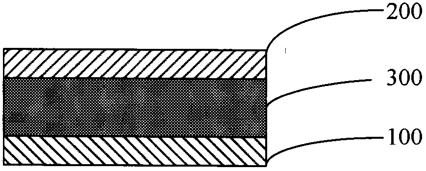
[0052] The overall structure of the resistive memory device of sample 1 is the same as that of the comparative sample, both of which are ITO / TiO 2 / ITO structure. The difference is that sample 1 is as follows Figure 3A The preparation method of the present invention described in is prepared at room temperature.
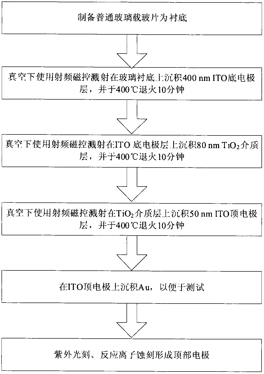
[0053] Such as Figure 3A As shown in the flow chart, first, 400nm ITO (bottom electrode layer), 80nm TiO were deposited layer by layer on a commercial ordinary glass slide using radio frequency magnetron sputtering 2 (dielectric layer), 50nm ITO (top electrode layer). Deposition of each layer was performed at relatively low temperature (temperature range from about 0°C to about 150°C, ie, without a high temperature annealing step after deposition. The deposition process is preferably carried out at room temperature, ie at a temperature around 25°C.
[0054] Similarly, for the convenience of testing, Au was further deposited on the...
Embodiment 2
[0056] Example 2 - Sample 2
[0057] Sample 2 has the same structure as sample 1, both are ITO / TiO 2 / ITO / . The difference lies in the preparation, the ITO bottom electrode is deposited at high temperature, and the dielectric layer TiO 2 and top electrode ITO are carried out at room temperature.
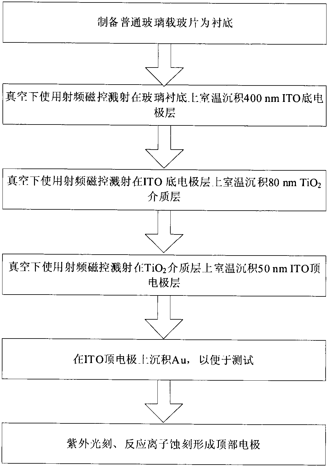
[0058] Such as Figure 3B The flow chart shown, first deposits 400nm ITO (bottom electrode) on a commercially available glass slide using RF magnetron sputtering, followed by annealing at 400°C for 10 minutes;
[0059] Afterwards, 80nm TiO was further deposited on the annealed ITO bottom electrode using RF magnetron sputtering. 2 Dielectric layer and 50nm ITO top electrode, the deposition of both the dielectric layer and the top electrode was carried out at room temperature (temperature range from about room temperature to about 150° C.), and there was no high temperature annealing step after deposition.
[0060] Au is then further deposited on the ITO top electrode, and when th...
Embodiment 3
[0061] Example 3 - Sample 3
[0062] Sample 3 was prepared in the same way as Sample 1. The only difference is that the dielectric layer of sample 3 uses MgO, and the preparation method of sample 3 is also the same as Figure 3A The preparation method of sample 1 in is similar, all carried out at room temperature.
[0063] First, 400nm ITO (bottom electrode layer), 80nm MgO (dielectric layer), and 50nm ITO (top electrode layer) were deposited layer by layer on a commercial common glass slide by radio frequency magnetron sputtering. Deposition of each layer is carried out at relatively low temperature (temperature range from about 0°C to about 150°C), ie without a high temperature annealing step after deposition, preferably at room temperature.
[0064] Similarly, for the convenience of testing, Au was further deposited on the top electrode ITO, and after the deposition was completed, the top electrode was formed using standard ultraviolet lithography and reactive ion etching...
PUM
| Property | Measurement | Unit |
|---|---|---|
| Thickness | aaaaa | aaaaa |
| Thickness | aaaaa | aaaaa |
Abstract
Description
Claims
Application Information
 - Generate Ideas
- Intellectual Property
- Life Sciences
- Materials
- Tech Scout
- Unparalleled Data Quality
- Higher Quality Content
- 60% Fewer Hallucinations
Browse by: Latest US Patents, China's latest patents, Technical Efficacy Thesaurus, Application Domain, Technology Topic, Popular Technical Reports.
© 2025 PatSnap. All rights reserved.Legal|Privacy policy|Modern Slavery Act Transparency Statement|Sitemap|About US| Contact US: help@patsnap.com