
Method for casting large-grained silicon ingot

A large-grain, silicon ingot technology, applied in chemical instruments and methods, crystal growth, single crystal growth, etc., can solve the problems affecting the photoelectric conversion rate of batteries, high photoelectric conversion rate of batteries, and high production costs

Inactive Publication Date: 2012-09-05
ZHENJIANG HUANTAI SILICON TECH
View PDF8 Cites 4 Cited by
  • Summary
  • Abstract
  • Description
  • Claims
  • Application Information

AI Technical Summary

Problems solved by technology

[0002] Polycrystalline silicon has a large number of grain boundaries, which affects the photoelectric conversion rate of the battery, while monocrystalline silicon has a relatively complete internal crystal structure and fewer defects, so the photoelectric conversion rate of the battery is high, but the production cost is higher.

Method used


Image

  • Method for casting large-grained silicon ingot
  • Method for casting large-grained silicon ingot
  • Method for casting large-grained silicon ingot

Examples


Embodiment Construction

[0017] The single crystal bar with (100) crystal orientation obtained by the Czochralski method is cut according to a certain direction to make a single crystal silicon plate as a seed crystal. The shape of the monocrystalline silicon plate can be a long plate with a length of 720mm-800mm, a width of 125mm-200mm, and a thickness of 10mm-30mm.

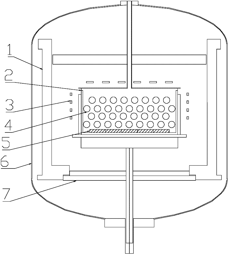
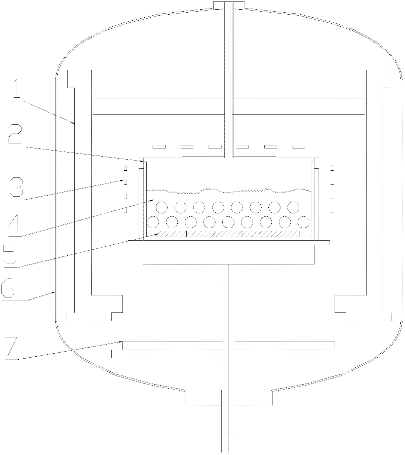
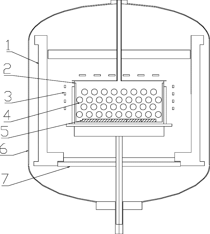
[0018] like figure 1 and figure 2 As shown, select a quartz crucible 2 of a standard size, select 5 above-mentioned monocrystalline silicon plates 5 and place them flat on the bottom of the crucible, and add an appropriate amount of doping elements such as boron or phosphorus according to the requirements of the target resistivity of 1-3 ohm / cm , fill the polysilicon material 4 above the single crystal plate 5; put the crucible 2 with the raw material into the polysilicon furnace 6, vacuumize and heat, and control the temperature of the heater 3 to be 1420-1550 ° C, so that the polysilicon on the upper part of the seed crystal The ma...


PUM


Abstract

The invention discloses a method for casting a large-grained silicon ingot by adopting a directional-solidification growing method, mainly comprising the following steps of: (1) putting a monocrystalline silicon plate cut according to a certain crystal orientation on the bottom layer of a quartz crucible as seed crystals; (2) filling an appropriate quantity of polycrystalline silicon materials and doping elements on the seed crystals; (3) putting the crucible with the raw materials into a polycrystalline furnace, vacuumizing and heating to melt the silicon material at the upper part, and when the monocrystalline silicon plate starts to be melted at the later stage of melting, the temperature of the bottom of the crucible is controlled by adjusting the rise height of a heat-resistant cage; therefore, the seed crystals are partially melted; and (4) staring a crystal growing procedure, and forming a vertical temperature gradient by controlling the power of a heater and lifting the heat-resistant cage, so that the silicon crystals grow in the direction of the monocrystalline silicon plate which is not completely melted; and finally, carrying out annealing and cooling steps to obtain the large-grained polycrystalline silicon ingot.

Description

technical field [0001] The invention belongs to the field of solar cell silicon chip manufacturing, and in particular relates to a method for casting large-grain silicon ingots. Background technique [0002] Polycrystalline silicon has a large number of grain boundaries, which affects the photoelectric conversion rate of the battery, while monocrystalline silicon has a relatively complete internal crystal structure and fewer defects, so the photoelectric conversion rate of the battery is high, but the production cost is higher. Contents of the invention [0003] The technical problem to be solved by the present invention is to provide a method for casting large-grain silicon ingots. This method utilizes the original low-cost and high-yield polysilicon casting technology to produce large-grain silicon ingots similar to single crystals and reduce grain boundaries. Quantity, improve the photoelectric conversion efficiency of the silicon wafer. [0004] In order to solve the ...

Claims


Application Information

Patent Timeline
Patent Type & Authority Applications(China)
IPC IPC(8): C30B11/00C30B28/06C30B29/06
Inventor 司荣进袁志钟王禄堡
Owner ZHENJIANG HUANTAI SILICON TECH
Learn More