
Method and device for growing silicon carbide crystal according to PVT (Physical Vapor Transport) method

A silicon carbide and crystal technology, applied in the field of growing silicon carbide crystals by PVT method, can solve various crystal defects and difficulties in growing high-quality crystals, etc.

Inactive Publication Date: 2012-08-22
吴晟
View PDF3 Cites 9 Cited by
  • Summary
  • Abstract
  • Description
  • Claims
  • Application Information

AI Technical Summary

Problems solved by technology

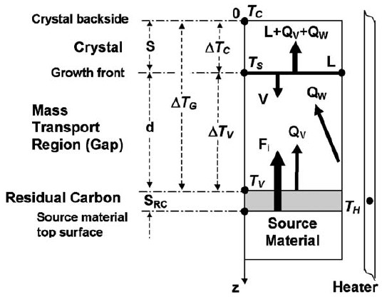
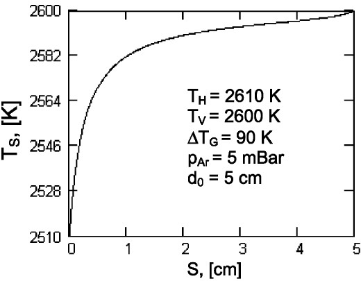
More importantly, the temperature of the crystallization interface, the crystallization driving force and the crystal growth rate are constantly changing throughout the growth process, and the instability of the growth process will inevitably lead to various crystal defects in the crystal, making it difficult to grow high-quality crystals

Method used


Image

  • Method and device for growing silicon carbide crystal according to PVT (Physical Vapor Transport) method
  • Method and device for growing silicon carbide crystal according to PVT (Physical Vapor Transport) method
  • Method and device for growing silicon carbide crystal according to PVT (Physical Vapor Transport) method

Examples


Embodiment 1

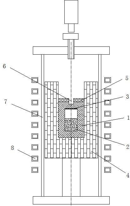
[0039] (1) if Figure 5 As shown, on the top of the graphite crucible cover, an adiabatic moving adjusting element 9 made of solid carbon (graphite) felt or soft (graphite) carbon felt is added to regulate the heat flow, and the movable adiabatic adjusting element 9 is suspended on the graphite The lower end of the connecting rod. The connecting rod is connected with the precision linear motion system installed outside the vacuum furnace described in the following (2) through the vacuum dynamic sealing junction. When growing crystals, the movable heat insulating adjustment element 9 can be moved according to the process requirements to change the heat preservation effect above the crucible to offset the influence of the increase in crystal thickness on the temperature of the growth surface.

[0040] (2) The equipment used in the embodiment such as Figure 5 As shown, it includes a vacuum chamber composed of a high-purity recrystallized alumina tube and upper and lower sealin...

Embodiment 2

[0058] (1) The growth equipment used in Example 2 is the same as that described in (1), (2), (3) and (4) in Example 1.

[0059] (2) The inner hole diameter of the graphite crucible used for crystal growth is 78mm, the inner hole height is 140mm, and the outer diameter is 140mm. It is made of high-purity, high-density, high-strength graphite.

[0060] Put 800 grams of silicon carbide polycrystalline powder with a particle size of 0.1 to 2 mm and a purity of more than 4 nines in the crucible.

[0061] The seed crystal used is a silicon carbide single wafer with a diameter of 76.2mm and a thickness of about 0.3-0.5mm, which is pasted on the inner surface of the upper cover of the graphite crucible.

[0062] The insulation parts on the periphery and bottom of the graphite crucible are made of high-purity solid carbon felt or soft carbon felt, with a diameter of 280--300mm and a height of 480mm. There is a hole coaxially in the middle for placing the graphite crucible: the diamete...

Embodiment 3

[0073] (1) The growth equipment used in Example 3 is the same as that described in (1), (2) and (3) in Example 1. However, a larger vacuum furnace and induction coil are used.

[0074] (2) The inner hole diameter of the graphite crucible used for crystal growth is 106, the inner hole height is 160mm, and the outer diameter is 190mm, which is made of high-purity, high-density, high-strength graphite.

[0075] Fill the crucible with 1600 grams of silicon carbide polycrystalline powder with a particle size of 0.1 to 2 mm.

[0076] The seed crystal used is a silicon carbide single wafer with a diameter of 101.6mm and a thickness of about 0.3-0.5mm, which is pasted on the inner surface of the upper cover of the graphite crucible.

[0077] The insulation parts on the periphery and bottom of the graphite crucible are made of high-purity solid carbon felt or soft carbon felt, with a diameter of 300mm and a height of 520mm. There is a hole for placing the graphite crucible coaxially ...


PUM

PropertyMeasurementUnit
heightaaaaaaaaaa
diameteraaaaaaaaaa
thicknessaaaaaaaaaa

Abstract

The invention relates to a method and a device for growing a silicon carbide crystal according to a PVT (Physical Vapor Transport) method. A moveable heat-insulating adjusting element is arranged above a crucible; when the silicon carbide crystal grows, with the thickening of the crystal on a crucible cover, a distance D between the moveable heat-insulating adjusting element and the crucible cover is gradually increased, wherein the thermal resistance Rc of the crystal to thermal flux Q is increased, with the increasing of the thickness of the crystal; the equivalent thermal resistance Rb of the moveable heat-insulating adjusting element to the thermal flux Q is reduced while the distance D is increased; and the temperature of a crystal interface is kept unchanged by keeping the dynamic balance between the increment of Rc and the reduction of Rb. According to the method, a heat-insulating adjusting element on the crucible cover is changed into the heat-insulating adjusting element which can move according to the technical demand during the growing process of the crystal. A geometric structure of a heat-insulating system and the energy output of a graphite crucible are changed by changing the distance between the moveable heat-insulating adjusting element and the crucible cover, so that the purpose of adjusting the temperature field in the graphite crucible during the growing process of the crystal is achieved.

Description

technical field [0001] The invention relates to a method and a device for growing silicon carbide crystals by a PVT method. Background technique [0002] Silicon carbide (SiC) single crystal has excellent semiconductor physical properties such as high thermal conductivity, high breakdown voltage, extremely high carrier mobility, and high chemical stability; it can be made into a high-frequency semiconductor that works under high temperature and strong radiation conditions. , High-power electronic devices and optoelectronic devices have great application value in the fields of national defense, high technology, industrial production, power supply, and transformation, and are regarded as the third-generation wide-bandgap semiconductor materials with great development prospects. However, it is very difficult to grow silicon carbide crystals. After years of hard work, the laboratory represented by Gree Company in the United States has successfully grown large-diameter high-quali...

Claims


Application Information

Patent Timeline
Patent Type & Authority Applications(China)
IPC IPC(8): C30B23/00C30B29/36
Inventor 吴晟
Owner 吴晟
Learn More