Method for improving write margin of static random access memory

A static random and write redundancy technology, applied in semiconductor/solid-state device manufacturing, electrical components, circuits, etc., can solve the problem that the write redundancy of static random access memory is not particularly ideal, and improve the write redundancy. , the effect of reducing hole mobility and increasing equivalent resistance

Inactive Publication Date: 2012-08-15
SHANGHAI HUALI MICROELECTRONICS CORP
View PDF4 Cites 2 Cited by
  • Summary
  • Abstract
  • Description
  • Claims
  • Application Information

AI Technical Summary

Problems solved by technology

[0005] However, the writing redundancy of the SRAM manufactured by the SRAM manufacturing method according to the prior art is not particularly ideal, so it is desired to provide a method for effectively improving the writing redundancy of the SRAM

Method used


Image

  • Method for improving write margin of static random access memory
  • Method for improving write margin of static random access memory
  • Method for improving write margin of static random access memory

Examples


Embodiment Construction

[0019] In order to make the content of the present invention clearer and easier to understand, the content of the present invention will be described in detail below in conjunction with specific embodiments and accompanying drawings.

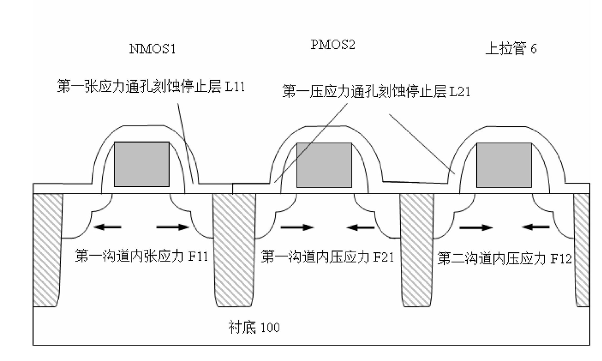
[0020] Specifically, refer to image 3 Let's first describe the prior art. image 3 It is a schematic diagram used in the process of the prior art. After the stress engineering treatment of the double stress via etch stop layer, the area NMOS1 of all NMOS devices covers the first stress via etch stop layer L11, and the area of ​​the pull-up tube 6 The region PMOS2 of all other PMOS devices (hereinafter referred to as “all other PMOS devices”) and the region of the pull-up tube 6 cover the first compressive via etch stop layer L21 .

[0021] Such as image 3 As shown, the NMOS device area is covered with a via etch stop layer (the first tensile stress via etch stop layer L11) that generates tensile stress, and the stress generated in the channe...


PUM


Abstract

The invention provides a method for improving a write margin of a static random access memory, which comprises the following steps: when a dual-stress through hole etch stop layer stress processing is adopted, the areas of all NMOS (N-channel metal oxide semiconductor) devices are covered by a tensile-stress through hole etch stop layer; the areas of all PMOS (P-channel metal oxide semiconductor) devices except a pull up MOS area are covered by a pressure-stress through hole etch stop layer; the pull up MOS area is covered by the tensile-stress through hole etch stop layer; and therefore the pull up MOS area and the areas of the NMOS devices keep the tensile stress. In the preparation process of the static random access memory, when dual-stress through hole etch stop layer stress engineering is adopted, a through hole etch stop layer capable of generating tensile stress in channels is used for the pull up MOS area, so that hole mobility of the pull up MOS is lowered, the equivalent resistance of the pull up MOS is increased, and the write margin of the static random access memory is improved.

Description

technical field [0001] The present invention relates to the technical field of semiconductor preparation, more precisely, the present invention relates to a method for improving the writing redundancy of SRAM, and the manufacture of SRAM using the method for improving the writing redundancy of SRAM method. Background technique [0002] Static random access memory (SRAM), as an important product in semiconductor memory, has been widely used in high-speed data exchange systems such as computers, communications, and multimedia. figure 1 What is shown is a layout structure of a common SRAM cell below 90 nanometers, including three levels of active regions, polysilicon gates, and contact holes. The area 1 marked in the figure is the control transistor (Pass Gate), which is an NMOS device, and the area 2 marked is the pull-down transistor (Pull Down MOS), which is also an NMOS device, and the area 3 is marked The one that comes out is the pull-up tube (Pull Up MOS), and the devi...

Claims


Application Information

Patent Timeline
Patent Type & Authority Applications(China)
IPC IPC(8): H01L21/8244
Inventor 俞柳江
Owner SHANGHAI HUALI MICROELECTRONICS CORP
Why Eureka
Try Eureka