Method for improving write redundancy of SRAM

A static random, write redundancy technology, applied in semiconductor/solid-state device manufacturing, semiconductor devices, electrical components, etc., can solve the problems of small write redundancy and low equivalent resistance, etc.

Active Publication Date: 2016-11-02
SHANGHAI HUALI MICROELECTRONICS CORP
View PDF7 Cites 0 Cited by
  • Summary
  • Abstract
  • Description
  • Claims
  • Application Information

AI Technical Summary

Problems solved by technology

However, in the existing SRAM, the equivalent resistance of the pull-up transistor is small, which leads to a small write margin (Write Margin) of the SRAM

Method used


Image

  • Method for improving write redundancy of SRAM
  • Method for improving write redundancy of SRAM
  • Method for improving write redundancy of SRAM

Examples


Embodiment Construction

[0024] In order to illustrate the technical content, structural features, achieved goals and effects of the present invention in detail, the following will be described in detail in conjunction with the embodiments and accompanying drawings.

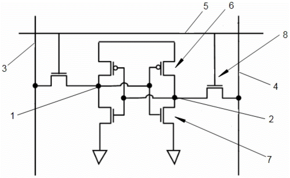
[0025] see figure 1 , figure 1 Shown is a schematic diagram of an equivalent circuit for writing in the SRAM of the present invention. Write margin (Write Margin) is an important parameter to measure the write performance of the SRAM unit. In the writing equivalent circuit of the SRAM, it is assumed that the first node 1 stores data at a low potential (that is, the stored data is "0"), and the second node 2 stores data at a high potential (that is, stores The data is "1"), non-limiting list, for example, writing a high potential to the first node 1, writing a low potential to the second node 2, before the writing action, the first bit line 3 will be precharged to a high potential, and the second bit line 4 will be precharged to a low ...


PUM


Abstract

A method for improving write redundancy of SRAM, comprising: step S1: providing a silicon-based substrate and forming shallow trench isolation; step S2: forming an NMOS device and a PMOS device as a pull-up transistor; step S3 : performing source-drain implantation in the source and drain regions of the NMOS device and the PMOS device as a pull-up transistor, and depositing a silicon nitride protective layer; step S4: performing source-drain implantation on the NMOS device and the PMOS device as a pull-up transistor Annealing process; step S5: removing the silicon nitride protection layer by etching. In the present invention, the PMOS device region and the NMOS device of the pull-up transistor are covered when preparing the photolithography plate of the stress memory effect process. In the stress memory effect process, both the pull-up transistor and the NMOS device are covered by a silicon nitride protective layer. Afterwards, the source-drain annealing process is performed, the hole mobility of the pull-up transistor is reduced, thereby increasing the equivalent resistance of the pull-up transistor, and during the writing process, the potential of the second node is lowered, thereby improving its writing redundancy.

Description

technical field [0001] The invention relates to the technical field of semiconductors, in particular to a method for improving write redundancy of a static random access memory. Background technique [0002] Static Random Access Memory (SRAM), as an important product in semiconductor memory, has been widely used in high-speed data exchange systems such as computers, communications, and multimedia. [0003] Generally, the layout of the SRAM below 90nm includes three levels of active area, polysilicon gate, and contact holes, and control transistors are respectively formed on the layout area, and the control transistors are NMOS devices; pull-down transistors (Pull Down MOS), the pull-down transistor is an NMOS device; the pull-up transistor (Pull Up MOS), the pull-up transistor is a PMOS device. However, in the existing SRAM, the equivalent resistance of the pull-up transistor is small, which leads to a small write margin (Write Margin) of the SRAM. Seeking a method for inc...

Claims


Application Information

Patent Timeline
Patent Type & Authority Patents(China)
IPC IPC(8): H01L21/8244
CPCH01L29/66568H01L29/7843H01L29/7847H10B10/12
Inventor 俞柳江
Owner SHANGHAI HUALI MICROELECTRONICS CORP
Why Eureka
Try Eureka