Method for improving write margin of static random access memory (SRAM)

A static random, write redundant technology, applied in semiconductor/solid-state device manufacturing, electrical components, circuits, etc., can solve problems such as reducing hole mobility, increase equivalent resistance, and improve write redundancy , the effect of reducing the potential

Active Publication Date: 2014-04-30
SHANGHAI HUALI MICROELECTRONICS CORP
View PDF3 Cites 0 Cited by
  • Summary
  • Abstract
  • Description
  • Claims
  • Application Information

AI Technical Summary

Problems solved by technology

However, the tensile stress in the channel will reduce the mobility of holes, so this method is generally not used for PMOS devices

Method used


Image

  • Method for improving write margin of static random access memory (SRAM)
  • Method for improving write margin of static random access memory (SRAM)
  • Method for improving write margin of static random access memory (SRAM)

Examples


Embodiment Construction

[0024] The present invention will be further described below in combination with principle diagrams and specific operation examples.

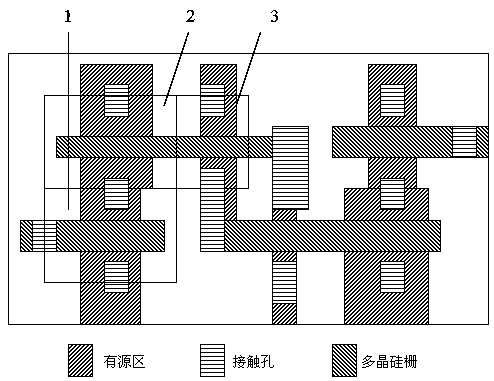
[0025] Such as Figure 4 Shown, the present invention improves the method for SRAM writing redundancy, and it comprises the following steps:

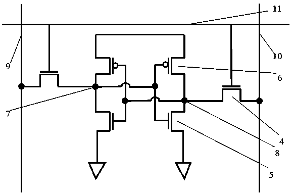
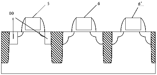
[0026] A SRAM substrate 0 is provided, and the substrate 0 includes sequentially adjacent NMOS regions 5, a first PMOS region 6 and a second PMOS region 6', and the first NMOS region 5 is used to prepare common NMOS devices, control transistors and pull-down tube, the first PMOS area is used to prepare a common PMOS device, and the second PMOS area is used to prepare a pull-up tube;

[0027] A shallow trench isolation region (STI) is respectively formed between the NMOS region 5, the first PMOS region 6 and the second PMOS region 6';

[0028] Simultaneously, a silicon carbide epitaxial formation process that generates tensile stress is adopted for the NMOS region 5 and the second PMOS region 6', and si...


PUM


Abstract

The invention discloses a method for improving write margin of a static random access memory (SRAM). The method comprises the following steps of: providing an SRAM substrate, wherein an N-channel metal oxide semiconductor (NMOS) area, a first P-channel metal oxide semiconductor (PMOS) area and a second PMOS area which are adjacent to each other are arranged on the substrate, the first NMOS area is used for manufacturing common NMOS devices, a pass gate and a pull down MOS, the first PMOS area is used for manufacturing common PMOS devices, and the second PMOS area is used for manufacturing a pull up MOS; forming a shallow trench isolation area among the NMOS area, the first PMOS area and the second PMOS area; and performing a SiC epitaxial formation process for generating tensile stress on the NMOS area and the second PMOS area, and epitaxially forming SiC lattices in the source and drain of the NMOS area and the second PMOS area respectively. By the method, the tensile stress of the pull up MOS in a trench direction is improved, the carrier mobility of a pull up MOS device is reduced, the equivalent resistance of the pull up MOS is increased, and the write margin of a random memory is improved.

Description

technical field [0001] The invention relates to the technical field of semiconductor preparation, in particular to a method for improving the writing redundancy of a SRAM. Background technique [0002] Static random access memory (SRAM), as an important product in semiconductor memory, has been widely used in high-speed data exchange systems such as computers, communications, and multimedia. figure 1 What is shown is the layout structure of a common SRAM cell below 90 nanometers, including three levels of active area, polysilicon gate, and contact hole. The area 1 in the figure is marked as the control tube (Pass Gate). The device is an NMOS device, and the one marked in area 2 is a pull-down transistor (Pull Down MOS), which is also an NMOS device, and the one marked in area 3 is a pull-up transistor (Pull Up MOS), and the device is a PMOS device. [0003] Write margin (Write Margin) is an important parameter to measure the write performance of SRAM cells. figure 2 It i...

Claims


Application Information

Patent Timeline
Patent Type & Authority Patents(China)
IPC IPC(8): H01L21/8244
Inventor 俞柳江
Owner SHANGHAI HUALI MICROELECTRONICS CORP
Why Eureka
Try Eureka