


Quick Research
Generate reliable direction feasibility study reports for your R&D in just a few steps.

Technical Q&A
Discover and master advanced knowledge NOW. Basics, ideas, possibilities, all at once.

Find Solutions
As an expert in R&D theories, this can generate solutions to your technical problems instantly.

Evaluate Feasibility
Analyze your overall solution with one click, know your potential R&D risks in advance.

Monitor Landscape
Get weekly tech updates, stay abreast of the latest tech innovations and key insights.
Memory unit and method of operating the same
A storage device, a technology in operation, applied in the direction of information storage, static memory, digital memory information, etc., can solve the problems of difficulty in improving data retention characteristics, difficulty in properly adjusting the balance of strength, etc., to improve long-term reliability and improve data retention characteristics Effect
- Summary
- Abstract
- Description
- Claims
- Application Information
AI Technical Summary
Problems solved by technology
Method used
Image


Examples
Embodiment approach
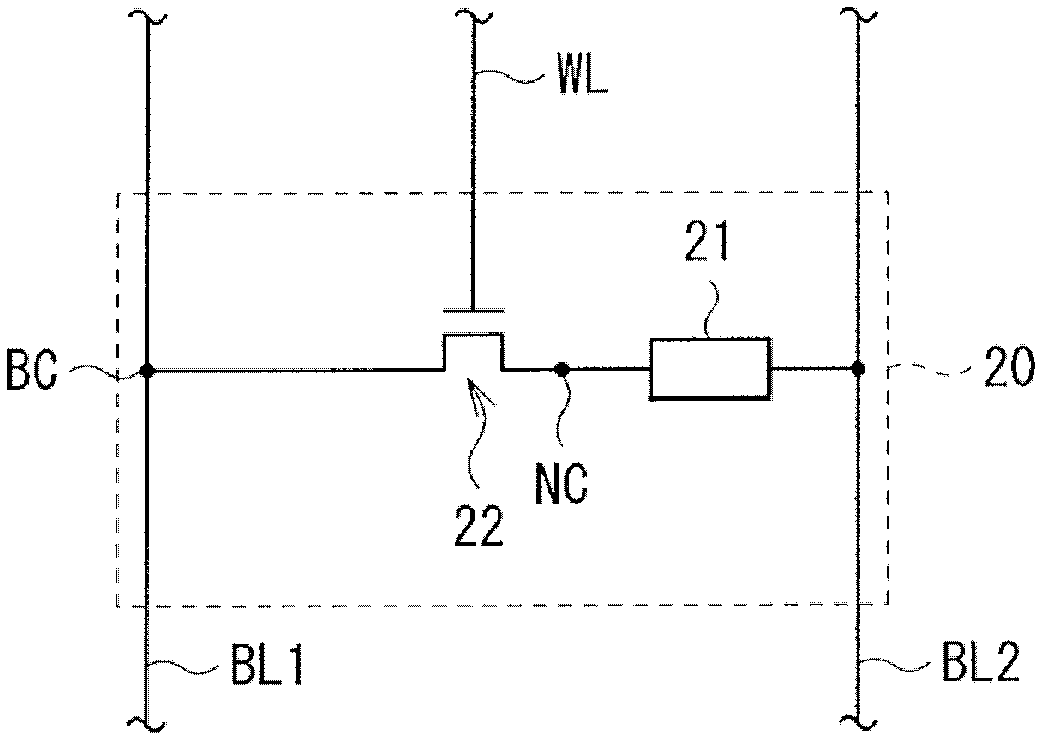
[0043] Structure of Storage Device 1
[0044] figure 1 A block diagram structure of a storage device (storage device 1 ) according to an embodiment of the present invention is illustrated. The memory device 1 includes a memory array 2 including a plurality of memory cells 20 , a word line driver 31 , and a bit line driver / sense amplifier 32 . The word line driver section 31 and the bit line driver section / sense amplifier 32 among the elements described above correspond to specific examples of the "driver section" in the present invention.
[0045] The word line drive section 31 applies a given potential (word line potential mentioned below) to a plurality (in this case, m pieces (m: an integer of 2 or more)) of word lines WL1 to WLm, which They are arranged parallel to each other (side by side) in the row direction.
[0046] The bit line driver / sense amplifier 32 applies a given potential to a plurality (m in this case) of bit lines BL11 to BL1m and a plurality (m in this c...
Deformed example 1
[0107] Figure 18 The setting operation and resetting operation of Modification 1 are illustrated with mode switching diagrams. specifically, Figure 18 State switching among four modes (operation modes) of A to D is illustrated.
[0108] Mode A is for performing the stepping operation ( Figure 12 to Figure 15 operation shown in C). Meanwhile, mode D is for performing the conventional general operation ( Figure 8A to Figure 9C operation shown in ) mode of operation. Furthermore, mode B is an operation mode for performing the stepping operation explained in the above-described embodiment in performing the setting operation and performing the conventional general operation explained in the above-described comparative example in performing the reset operation. In contrast, mode C is an operation mode for performing the stepping operation explained in the above embodiment in performing the reset operation and performing the conventional general operation explained in the ab...
Deformed example 2
[0113] Figure 19 A cross-sectional structure of a memory element (memory element 21A) according to Modification 2 is shown in the figure. The memory element 21A of this modified example is constituted by a phase change memory (Phase Change Memory, PCM).
[0114] The memory element 21A has between the lower electrode 211 and the upper electrode 213 made of, for example, Ge 2 Sb 2 Te 5 The storage layer 214 is made of such as GeSbTe alloy. In the memory layer 214, a phase transition from a crystalline state to an amorphous state or from an amorphous state to a crystalline state occurs by applying an electric current. In association with the phase transition described above, the resistance value (resistance state) undergoes an inversion change.
[0115] In the memory element 21A of this modified example, when a positive voltage or a negative voltage is applied between the lower electrode 211 and the upper electrode 213, the memory layer 214 changes from a high-resistance am...
PUM
 Abstract
Description
Claims
Application Information
 - R&D Engineer
- R&D Manager
- IP Professional
- Industry Leading Data Capabilities
- Powerful AI technology
- Patent DNA Extraction
Browse by: Latest US Patents, China's latest patents, Technical Efficacy Thesaurus, Application Domain, Technology Topic, Popular Technical Reports.
© 2024 PatSnap. All rights reserved.Legal|Privacy policy|Modern Slavery Act Transparency Statement|Sitemap|About US| Contact US: help@patsnap.com