Manufacturing method of STI (shallow trench insulation)

A manufacturing method and technology of shallow trenches, applied in semiconductor/solid-state device manufacturing, electrical components, circuits, etc., can solve problems such as boron ion concentration reduction and impact on NMOS device performance, and achieve the effect of avoiding threshold voltage drop

Active Publication Date: 2014-03-26
SEMICON MFG INT (SHANGHAI) CORP +1
View PDF3 Cites 0 Cited by
  • Summary
  • Abstract
  • Description
  • Claims
  • Application Information

AI Technical Summary

Problems solved by technology

[0015] In view of this, the technical problem solved by the present invention is: boron ions doped in the active region of the NMOS device easily diffuse into the silicon dioxide of shallow trench isolation during the annealing process of forming the P well, causing boron ions in the P well to The decrease of concentration and the drop of threshold voltage affect the performance of NMOS devices

Method used


Image

  • Manufacturing method of STI (shallow trench insulation)
  • Manufacturing method of STI (shallow trench insulation)
  • Manufacturing method of STI (shallow trench insulation)

Examples


Embodiment Construction

[0031] In order to make the object, technical solution, and advantages of the present invention clearer, the present invention will be further described in detail below with reference to the accompanying drawings and examples.

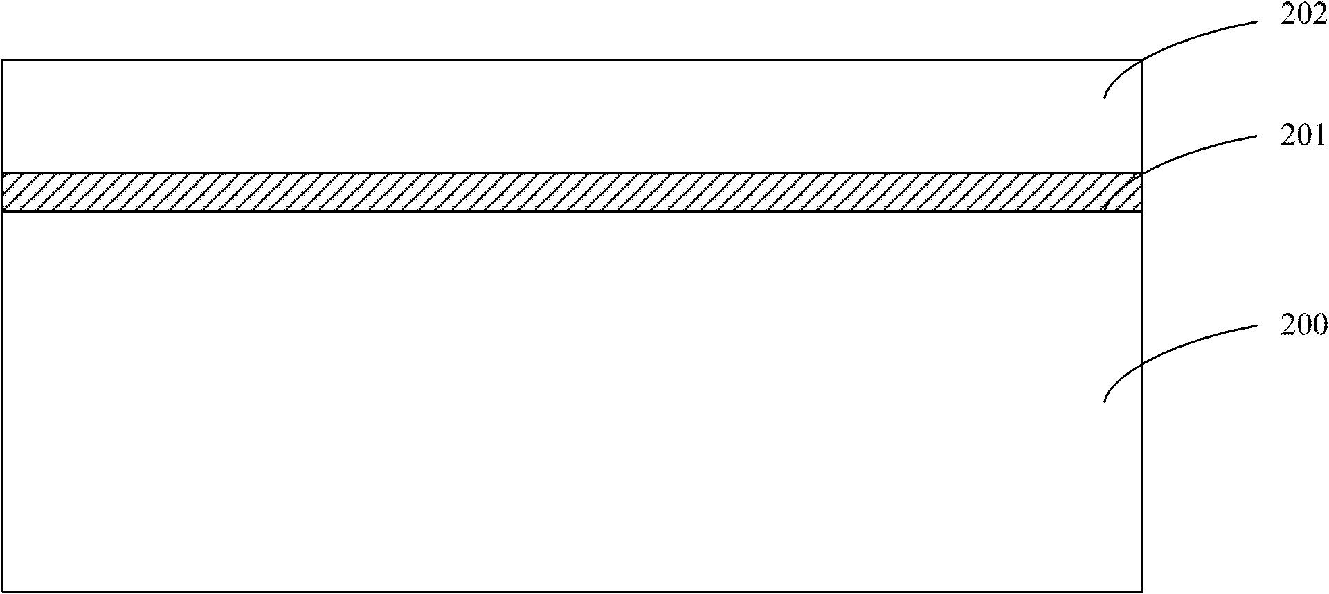
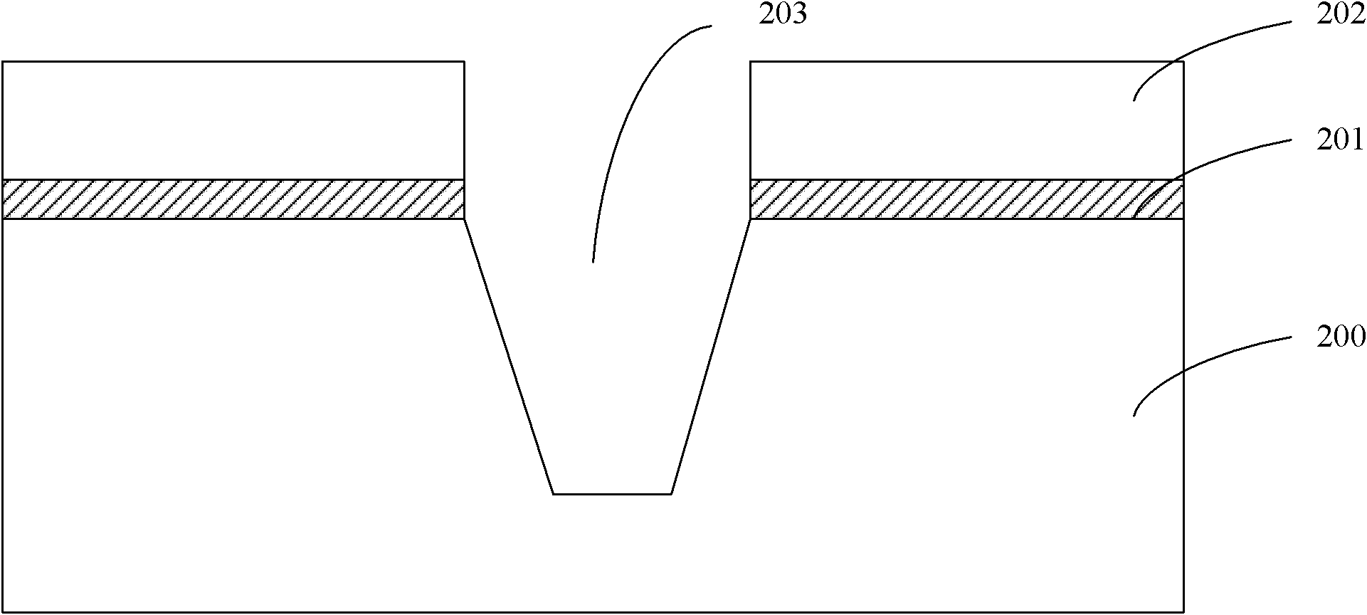
[0032] Provide a wafer with a silicon substrate, the silicon substrate can be an n-type substrate whose doping type is electron type or a p-type substrate whose doping type is hole type, combined Figure 8-14 ,Detailed description Figure 7 The shallow trench isolation manufacturing method of the present invention shown has the following steps:

[0033] Step 701, Figure 8 It is a schematic cross-sectional structure diagram of step 701 of the STI manufacturing method in the present invention, such as Figure 8 As shown, a silicon dioxide liner 201 and a silicon nitride layer 202 are sequentially deposited on the device surface of the wafer;

[0034] In this step, the silicon dioxide liner 201 and the silicon nitride layer 202 are sequentially deposite...


PUM

PropertyMeasurementUnit
thicknessaaaaaaaaaa

Abstract

The invention provides a manufacturing method of STI (shallow trench insulation). The method comprises the following steps: firstly growing an LO (lining oxide) on the surface of a shallow trench which is formed in a substrate through etching, and then carrying out primary boron element doping and secondary nitrogen element doping on the LO; forming a first barrier layer with boron ion concentration which is 1-2 orders of magnitude higher than a P well at the part, adjacent to the substrate region, of the LO; forming a second barrier layer above the first barrier layer; and finally, depositing silicon oxide in the shallow trench, carrying out CMP(chemical mechanical polishing) and STI annealing, thus forming the STI. The manufacturing method provided by the invention utilizes the second barrier layer to block boron ions in the first barrier layer so as to keep the concentration of the boron ions in the first barrier layer; the concentration of the boron ions in the first barrier layer is higher than the P well, in a follow-up P well annealing process, and the first barrier layer can be used for effectively preventing the boron ions in the P well from passing through the LO so as to diffuse into the STI; and the concentration of the boron ions injected into the P well is kept, and the performance of an NMOS (N-channel mental-oxide-semiconductor) device is prevented from being influenced by the degression of a threshold voltage caused by the reduction of the concentration of the boron ions.

Description

technical field [0001] The invention relates to a semiconductor manufacturing method, in particular to a shallow trench isolation manufacturing method. Background technique [0002] Current semiconductor integrated circuit (IC) devices are generally fabricated on a substrate. IC devices typically include various discrete circuit elements. In order to isolate discrete circuit components so that each discrete circuit component can work independently and will not be affected by the state of other components, before making IC devices, the substrate is first isolated from each other as active areas (Active Area, AA), Then make the discrete circuit components in AA. With the improvement of the integration level of IC devices, shallow trench isolation (Shallow Trench Insulation, STI) technology is usually used to form STI in the substrate. A typical discrete circuit element is a Metal-Oxide Semiconductor Field Effect Transistor (MOS) device. The structure of the MOS device incl...

Claims


Application Information

Patent Timeline
Patent Type & Authority Patents(China)
IPC IPC(8): H01L21/762H01L21/265
Inventor 赵猛
Owner SEMICON MFG INT (SHANGHAI) CORP
Why Eureka
Try Eureka