
Silicon-based integrated two-position binary electro-optical encoder

An encoder and binary technology, applied in the field of electro-optical encoder, can solve the problems of gate delay competition and risk, speed bottleneck, low cost, etc., and achieve the effect of high-speed and large-capacity information processing, fast speed, and fast encoding speed

Inactive Publication Date: 2012-06-27
INST OF SEMICONDUCTORS - CHINESE ACAD OF SCI
View PDF5 Cites 8 Cited by
  • Summary
  • Abstract
  • Description
  • Claims
  • Application Information

AI Technical Summary

Problems solved by technology

[0006] The main purpose of the present invention is to provide a silicon-based integrated two-bit binary electro-optic encoder to solve the speed bottleneck, power consumption, gate delay and the competition and risks brought by the gate delay in the traditional electrical encoder and other issues, in order to expect to play an important role in future photonic computers and optical computing, and use modern process technology to keep the device small size, low power consumption and low cost

Method used


Image

  • Silicon-based integrated two-position binary electro-optical encoder
  • Silicon-based integrated two-position binary electro-optical encoder
  • Silicon-based integrated two-position binary electro-optical encoder

Examples


Embodiment Construction

[0023] In order to make the objectives, technical solutions and advantages of the present invention clearer, the present invention will be further described in detail below with reference to specific embodiments and accompanying drawings.

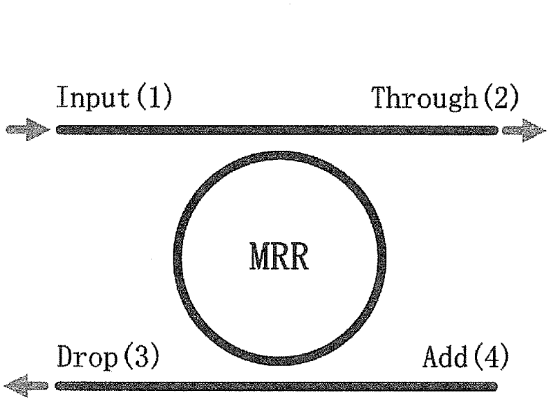
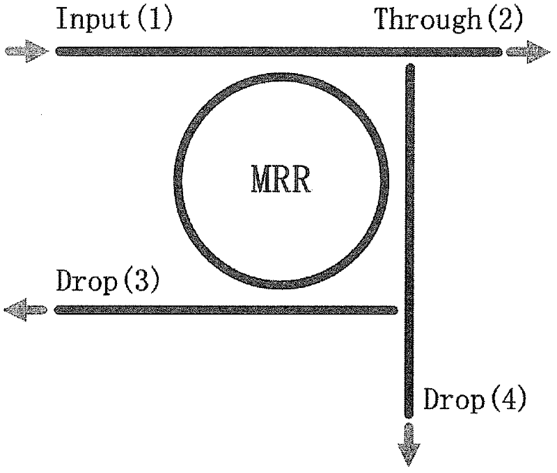
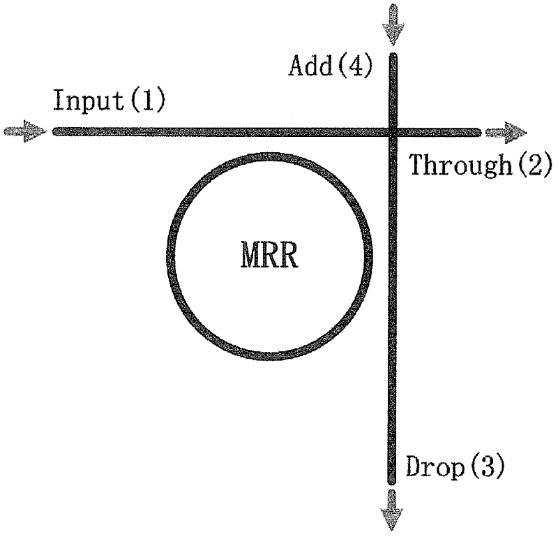
[0024] The invention discloses a silicon-based integrated two-bit binary electro-optical encoder, the basic structure of which is an optical switch based on a micro-ring resonator, and is made of a silicon-based nanowire waveguide. The electro-optical encoder is composed of three ring waveguides and three curved waveguides (theoretically four ring waveguides, one of which is virtual), it has four electrical signals and one continuous optical signal input at the working wavelength, The output is an optical signal. It is assumed that the microring resonator resonates when the modulation voltage applied to the microring is at a high level, and the microring resonator does not resonate at a low level, then the optical code of the four-bit elect...


PUM


Abstract

The invention relates to the technical field of electro-optical encoders, and discloses a silicon-based integrated two-position binary electro-optical encoder. The electro-optical encoder is realized by three micro-ring resonators (MRR) and three bent nanowire waveguides, wherein an input comprises four electric signals to be encoded and a continuous optical signal at a working wavelength; and an output result is an optical signal obtained by encoding the electric signal. The encoder can be used for finishing conversion between the electric signal and the optical signal, and the electric signal can be optically encoded. In the structure, each optical switch based on the micro-ring resonator is independent, and all the switches work in parallel at the same time; the encoding speed of the whole device is much quicker than that of an electric encoder. In the aspect of process, the conventional complementary metal-oxide-semiconductor (CMOS) technical process is used, so that the device has a small volume, low power consumption, high speed and high expandibility, is integrated with an electric element conveniently, and has a good application prospect in photon computers and optical communication networks.

Description

technical field [0001] The invention relates to the technical field of electro-optical encoders, in particular to a silicon-based integrated two-bit binary electro-optical encoder, which is particularly suitable for future photonic computers and optical communication networks. Background technique [0002] Existing computers transmit and process information electronically. With the advancement of semiconductor process technology, the size of transistors on a chip is getting smaller and smaller, and the number of transistors that can be integrated is increasing. In this way, the CPU can obtain a higher main frequency, but the most serious problem from the higher main frequency band is the sharp increase in power consumption, and the problems of leakage and heat dissipation cannot be solved. In terms of the development of high-speed computers, the use of electrons as information carriers can no longer meet people's requirements for faster processing speed of computers, and im...

Claims


Application Information

Patent Timeline
IPC IPC(8): H03M5/02
Inventor 田永辉杨林
Owner INST OF SEMICONDUCTORS - CHINESE ACAD OF SCI
Learn More