Metal insulation chip test needle frame
A technology of chip testing and metal insulation, applied in the direction of measuring electricity, measuring devices, measuring electrical variables, etc., can solve the problems that the coaxial controllable reactance chip test needle frame is not widely used, and the assembly and disassembly are inconvenient, etc., to achieve The effect of improving electrical performance and avoiding short circuit
- Summary
- Abstract
- Description
- Claims
- Application Information
AI Technical Summary
Problems solved by technology
Method used
Image
Examples
Embodiment 1
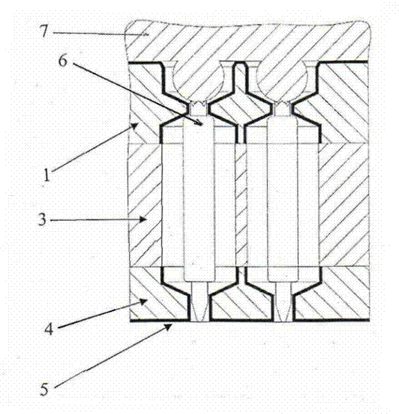
[0018] Example 1, such as figure 1 As shown, a metal-insulated chip test needle frame, the bottom is a probe holding plate 4 made of metal, and a spring probe 6 is inserted into the probe holding plate 4 . The ground copper block 3 is connected with the probe holding plate 4 , and the probe / chip positioning plate 1 made of metal is connected with the ground copper block 3 . The spring probe 6 is fixed on the probe holding plate 4 and put into the hole of the probe / chip positioning plate 1, and the upper end of the spring probe 6 is in contact with the chip to be tested. Through the metal aluminum oxidation process and Teflon spraying process, an insulating coating is formed on the inner wall and side of the probe holding plate 4 and the probe / chip positioning plate 1. The insulating coating is composed of aluminum oxide and Teflon. The thickness of the aluminum layer is 0.04 mm, and the thickness of the Teflon layer is 0.002 mm. At this time, the ratio of the inner diameter ...
Embodiment 2
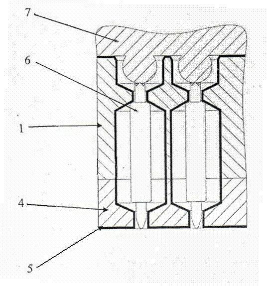
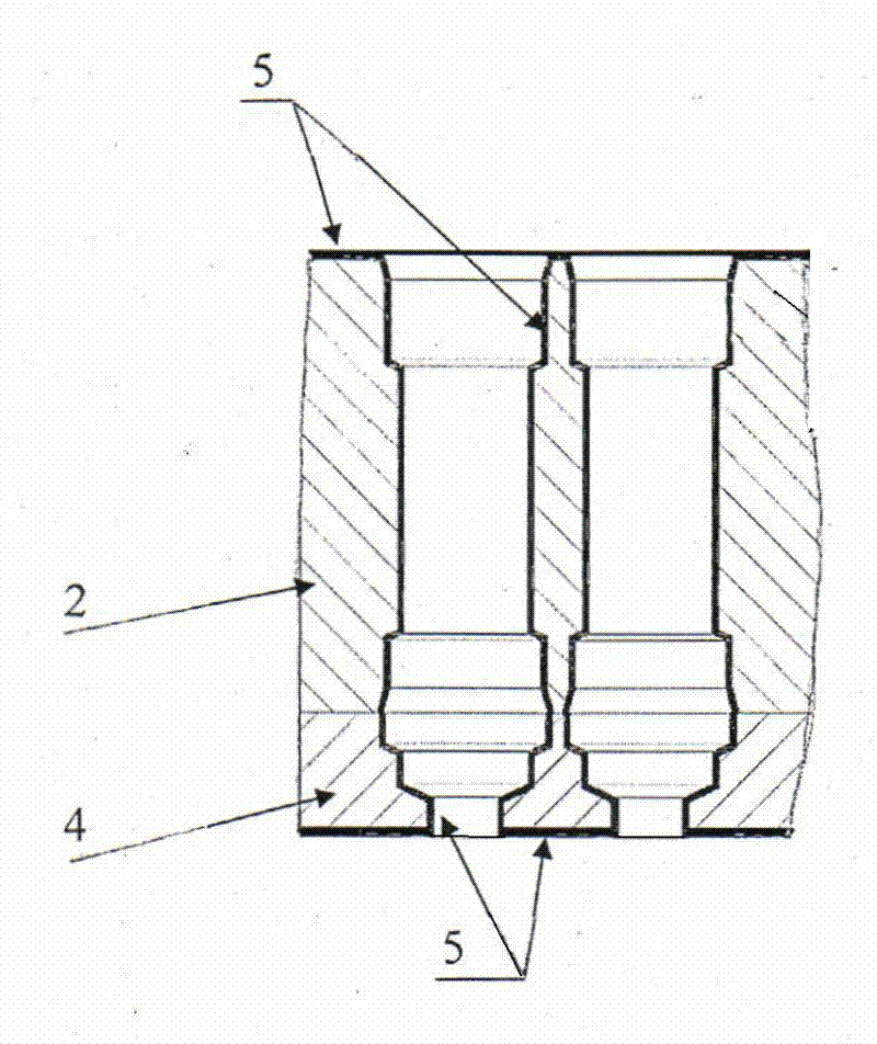
[0019] Example 2. If figure 2 with image 3 As shown, a metal-insulated chip test needle holder, the bottom is a probe holding plate 4 made of metal, and one end of a spring probe 6 is inserted into the probe holding plate 4 . Connected to the probe holding plate 4 is a metal probe / chip positioning plate 1 (see figure 2 ), or the needle holder body 2 made of metal (see image 3 ). The other end of the spring probe 6 is placed into the hole of the probe / chip positioning plate 1, and its upper end is in contact with the chip to be tested. Through metal aluminum oxidation process and Teflon spraying process, aluminum oxide and Teflon insulating coating are formed on the inner wall and side of probe holding plate 4, probe / chip positioning plate 1 (or needle frame main body 2). The layer is composed of alumina and Teflon, the thickness of the alumina layer is 0.02 mm, and the thickness of the Teflon layer is 0.001 mm. After having this insulating coating, the inner insulatio...
PUM
 Abstract
Description
Claims
Application Information
 - R&D
- Intellectual Property
- Life Sciences
- Materials
- Tech Scout
- Unparalleled Data Quality
- Higher Quality Content
- 60% Fewer Hallucinations
Browse by: Latest US Patents, China's latest patents, Technical Efficacy Thesaurus, Application Domain, Technology Topic, Popular Technical Reports.
© 2025 PatSnap. All rights reserved.Legal|Privacy policy|Modern Slavery Act Transparency Statement|Sitemap|About US| Contact US: help@patsnap.com


