Vertical parasitic pnp transistor in silicon germanium hbt process and manufacturing method thereof

A PNP triode and vertical parasitic technology, which is applied in semiconductor/solid-state device manufacturing, electrical components, circuits, etc., can solve the problems of large device area, device size reduction, and large collector connection resistance, so as to reduce collector resistance, Improved performance and reduced area

Active Publication Date: 2014-10-08
SHANGHAI HUAHONG GRACE SEMICON MFG CORP
View PDF7 Cites 0 Cited by
  • Summary
  • Abstract
  • Description
  • Claims
  • Application Information

AI Technical Summary

Problems solved by technology

The disadvantage is that the device area is large and the connection resistance of the collector is large
Since the extraction of the collector electrode in the prior art is realized through another active region adjacent to the collector region, and the other active region and the collector region need to be isolated by STI or other field oxygen, such This greatly limits the further reduction of the device size

Method used


Image

  • Vertical parasitic pnp transistor in silicon germanium hbt process and manufacturing method thereof
  • Vertical parasitic pnp transistor in silicon germanium hbt process and manufacturing method thereof
  • Vertical parasitic pnp transistor in silicon germanium hbt process and manufacturing method thereof

Examples


Embodiment Construction

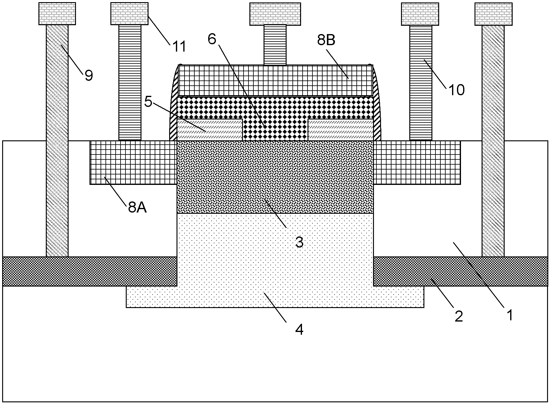
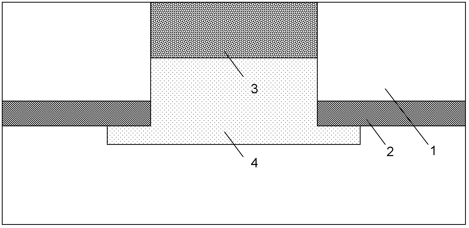
[0038] Such as figure 1 Shown is a schematic structural diagram of a vertical parasitic PNP transistor in the silicon germanium HBT process of the embodiment of the present invention. In the silicon germanium HBT process of the embodiment of the present invention, the vertical parasitic PNP transistor is formed on the silicon substrate, and the active region is isolated by the shallow trench field oxygen 1 .

[0039]The base region 3 of the PNP transistor is composed of an N-type ion implantation region formed in the active region. The process conditions of the N-type ion implantation in the base area are as follows: the implanted impurity is phosphorus or arsenic, the energy condition is 100Kev-300Kev, and the dose is 1e14cm -2 ~1e16cm -2 .

[0040] A groove in contact with the base region 3 is formed in the shallow groove field oxygen 1 on the peripheral side of the base region 3, and the shallow groove field oxygen 1 located in the groove is removed, and the The depth o...


PUM


Abstract

The invention discloses a vertical parasitic positive-negative-positive (PNP) triode in a SiGe heterojunction bipolar transistor (HBT) process. A slot which is contacted with a base region is formed in shallow slot field oxides around the base region, and the depth of the slot is less than or equal to that of the base region; polycrystalline silicon which is doped with N-type impurities is filled in the slot and forms an external base region; the external base region and the base region are contacted on the side of the base region; and metal contact is formed on the external base region and a base is led out. The invention also discloses a manufacturing method for the vertical parasitic PNP triode in the SiGe HBT process. The vertical parasitic PNP triode can be used as an output device in a high-speed and high-gain HBT circuit, one more device choice is provided for a circuit, the device area can be effectively reduced, the parasitic effect of the device can be reduced, the collector resistance of a PNP tube is reduced and the performance of the device is improved; and in the method, extra process conditions are not needed and production cost can be reduced.

Description

technical field [0001] The invention relates to the field of semiconductor integrated circuit manufacturing, in particular to a vertical parasitic PNP triode in the silicon germanium HBT process, and also relates to a method for manufacturing the vertical parasitic PNP triode in the silicon germanium HBT process. Background technique [0002] In RF applications, higher and higher device characteristic frequencies are required. In BiCMOS process technology, NPN transistors, especially silicon germanium (SiGe) heterojunction transistors (HBT) or germanium silicon carbon heterojunction transistors (SiGeC HBT) are good choices for UHF devices. And the SiGe process is basically compatible with the silicon process, so SiGe HBT has become one of the mainstreams of UHF devices. In this context, the requirements for the output device are correspondingly increased, such as having a certain current gain coefficient and cut-off frequency of not less than 15. [0003] In the prior art,...

Claims


Application Information

Patent Timeline
Patent Type & Authority Patents(China)
IPC IPC(8): H01L29/737H01L29/06H01L21/331
Inventor 陈帆陈雄斌薛凯周克然潘嘉李昊陈曦蔡莹
Owner SHANGHAI HUAHONG GRACE SEMICON MFG CORP
Why Eureka
Try Eureka