Nanocrystalline nickel with high-density twin structure and preparation method thereof
A nanocrystalline, high-density technology, applied in the field of nanocrystalline nickel material and its preparation, can solve the problem of not giving the proportion and content of nanotwin structure, and achieve the effects of wide application, simple preparation process and fast deposition rate.
- Summary
- Abstract
- Description
- Claims
- Application Information
AI Technical Summary
Problems solved by technology
Method used
Image
Examples
Embodiment 1
[0028] 1) Preparation of nano-twin crystal nickel material by electrolytic deposition technology
[0029] Electrolytic deposition equipment: DC electrolytic deposition power supply
[0030] Electrolyte ratio: 250 / L NiSO 4 +15g / L NiCl 2 +40g / L H 3 BO 3 Ionized water is used for distributing the electrolyte, and the acidity of the electrolyte is: pH=2.
[0031] Cathode and anode requirements: the anode is 99.97% pure nickel plate, and the cathode is stainless steel plate after degreasing treatment.
[0032] 2) Electrolysis process parameters: DC current density is 15A / dm 2, DC electroplating; the deposition time is 30min, the distance between cathode and anode is 15cm, and the area ratio of cathode and anode is 40:1; the electrolysis temperature is 25°C, and the electrolyte is stirred by electromagnetic stirring.
[0033] 3) A nickel material with nanoscale twin crystals is prepared. Figure 1 is an electron micrograph of the nano-twinned nickel material. The sample is comp...
Embodiment 2
[0035] 1) Preparation of nano-twin crystal nickel material by electrolytic deposition technology:
[0036] Electrolyte ratio: 350 / L NiSO 4 +10g / L NiCl 2 +30g / L H 3 BO 3 The acidity of the electrolyte is pH=2.5; the anode uses a pure nickel plate with a purity higher than 99.9%, the cathode uses a pure copper plate that has been pickled and degreased, and the area ratio of the anode and cathode is 30:1.
[0037] 2) Electrolysis process parameters: DC current density is 10A / dm 2 , DC electroplating; the deposition time is 15min, the distance between the cathode and the anode is 10cm, the electrolysis temperature is 20°C, and the electrolyte is stirred by electromagnetic means.
[0038] 3) Preparation of nickel material with nanoscale twin crystals, Figure 4 It is an electron micrograph of the nano-twinned nickel material. The sample is composed of nearly equiaxed submicron grains, and there are high-density twinned lamellar structures with different orientations inside the...
Embodiment 3
[0040] 1) Preparation of nano-twin crystal nickel material by electrolytic deposition technology:
[0041] Electrolyte ratio: 250g / L NiSO 4 +35g / LH 3 BO 3
[0042] The acidity of the electrolyte is pH=1; the anode is a 99.9% pure nickel plate, the cathode is a pure copper plate that has been pickled and degreased, and the area ratio of the anode and cathode is 50:1.
[0043] 2) Electrolysis process parameters: DC current density is 40A / dm 2 , DC electroplating; the deposition time is 30min, the distance between cathode and anode is 15cm, and the area ratio of cathode and anode is 50:1; the electrolysis temperature is 60°C, and the electrolyte is stirred by electromagnetic stirring.
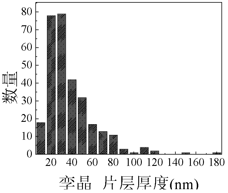
[0044] Under this process, nickel materials with a grain size between 20nm and 300nm and a twin-lamellar thickness between 20nm and 50nm can also be prepared. In the sample, the grains with the twin-lamellar structure account for 100% of the entire sample.
[0045] The sample has a yield stre...
PUM
| Property | Measurement | Unit |
|---|---|---|
| Average grain size | aaaaa | aaaaa |
| Thickness | aaaaa | aaaaa |
| Yield strength | aaaaa | aaaaa |
Abstract
Description
Claims
Application Information
 - R&D
- Intellectual Property
- Life Sciences
- Materials
- Tech Scout
- Unparalleled Data Quality
- Higher Quality Content
- 60% Fewer Hallucinations
Browse by: Latest US Patents, China's latest patents, Technical Efficacy Thesaurus, Application Domain, Technology Topic, Popular Technical Reports.
© 2025 PatSnap. All rights reserved.Legal|Privacy policy|Modern Slavery Act Transparency Statement|Sitemap|About US| Contact US: help@patsnap.com


