Image sensor

An image sensor and pixel technology, applied in the direction of semiconductor devices, electrical components, circuits, etc., can solve the problems of small depletion region width, reduced photodiode light absorption efficiency, photodiode parasitic effect radiation resistance, etc., to achieve small parasitic capacitance, The effect of reducing the probability of soft errors and improving the radiation resistance

Active Publication Date: 2014-01-08
河北苏格医疗科技有限公司
View PDF6 Cites 0 Cited by
  • Summary
  • Abstract
  • Description
  • Claims
  • Application Information

AI Technical Summary

Problems solved by technology

In Chinese invention patent 200910083526.X, the photodiode is still formed on the silicon substrate. The reason is that the structure of the photodiode is a vertical structure. Since the thickness of the top layer of silicon is relatively thin, the photodiode with the vertical structure is formed on a thinner substrate. In the top layer of silicon, the width of the depletion region formed when the photodiode is reverse-biased, that is, when the reverse bias voltage is added, is small, which reduces the light absorption efficiency of the photodiode.
However, although the above-mentioned patent can make other circuits outside the CMOS image sensor photodiode have the advantages of high speed, low power consumption, anti-lockup and low soft error probability, since the photodiode is still formed in the silicon substrate, the photodiode also has the advantages of Parasitic Effects and Issues with Radiation Resistance

Method used


Image

  • Image sensor
  • Image sensor
  • Image sensor

Examples


Embodiment Construction

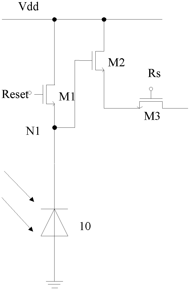
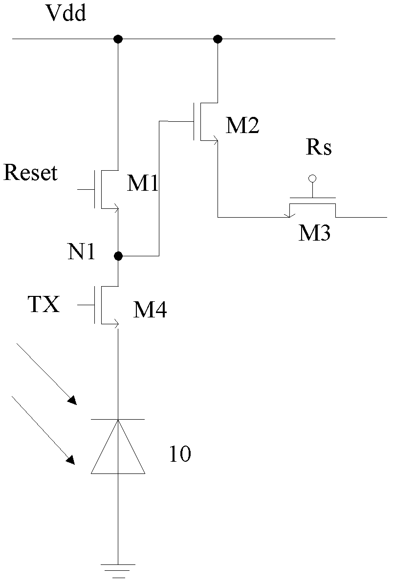
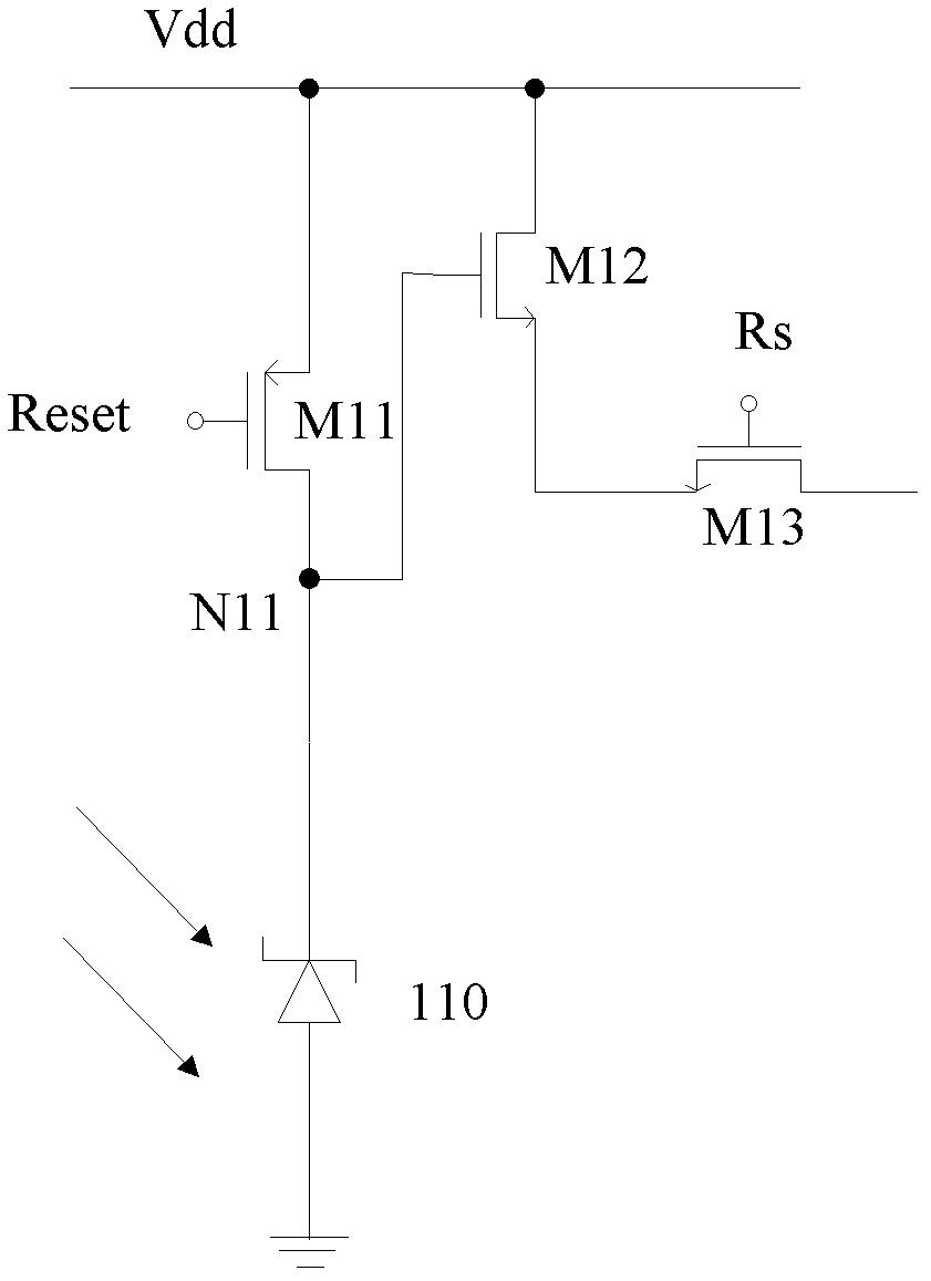
[0037] Such as image 3 Shown is an equivalent circuit structure diagram of a pixel unit circuit of an image sensor according to an embodiment of the present invention; the pixel unit circuit of an image sensor according to an embodiment of the present invention has a 3T structure. A pixel unit circuit of an image sensor according to an embodiment of the present invention includes a photosensitive structure 110 and a CMOS pixel readout circuit with a 3T structure.

[0038] Such as Figure 5 Shown is a cross-sectional view of the photosensitive structure 110 in Embodiment 1 of the present invention. In Embodiment 1 of the present invention, the pixel unit circuit and the CMOS digital-analog circuit of the CMOS image sensor are all formed on the top semiconductor layer 102 of the semiconductor substrate with an insulating buried layer, Figure 4 shows that the semiconductor substrate with an insulating buried layer includes a top semiconductor layer 102 , an insulating layer 1...


PUM


Abstract

The invention discloses an image sensor. Both a light sensing structure and a pixel reading circuit are formed on a top semiconductor layer of a semiconductor substrate with an insulating buried layer. The light sensing structure comprises three doped regions which are transversely arranged; a medium layer with non-uniform thickness is formed on an exhaustion region; and a polycrystal silicon layer is formed on the medium layer. The doped regions of the light sensing structure are transverse structures and can make the width of the exhaustion region break through the limitation of the thickness of the top semiconductor layer of a silicon on insulator (SOI), so that the light absorbency of the light sensing structure can be improved; the non-uniform medium layer which is formed on the exhaustion region and the polycrystal silicon layer can modulate the energy band of the exhaustion region to make the energy band of the exhaustion region steeper, so that the transfer efficiency of light-induced charges in the exhaustion region can be obviously increased; and the parasitic effect of the image sensor can be reduced and the radiation-resistant capability of the image sensor can be improved.

Description

technical field [0001] The present invention relates to an image sensor. Background technique [0002] In the 1970s, CCD image sensors and CMOS image sensors started at the same time. CCD image sensor has gradually become the mainstream of image sensor due to its high sensitivity and low noise. However, due to technological reasons, sensitive components and signal processing circuits cannot be integrated on the same chip, resulting in a camera assembled from a CCD image sensor with large volume and high power consumption. CMOS image sensor has been more and more widely used due to its advantages of high integration, low power and low cost. [0003] Existing CMOS image sensors include CMOS digital-analog circuits and pixel unit circuit arrays. According to the number of transistors included in one pixel unit circuit, existing CMOS image sensors are divided into 3T-type structures and 4T-type structures, and 5T-type structures can also be used. type structure. [0004] Suc...

Claims


Application Information

Patent Timeline
Patent Type & Authority Patents(China)
IPC IPC(8): H01L27/146H01L31/0352H01L31/0224
Inventor 汪辉林琳陈杰汪宁尚岩峰
Owner 河北苏格医疗科技有限公司
Why Eureka
Try Eureka