
Method for making V-shaped groove texture surface on surface of monocrystalline silicon solar cell

A technology for solar cells and monocrystalline silicon, applied in chemical instruments and methods, circuits, crystal growth, etc., can solve the problems of uneven inner surface, easy contamination of silicon wafers, low processing efficiency, etc., and achieve quality improvement and texturing efficiency. High, yield-enhancing effect

Inactive Publication Date: 2013-03-20
HENAN UNIV OF SCI & TECH
View PDF6 Cites 0 Cited by
  • Summary
  • Abstract
  • Description
  • Claims
  • Application Information

AI Technical Summary

Problems solved by technology

The mechanical groove method and laser groove method are characterized by controllable groove position and scale, but the inner surface of the groove is often undulating, which is easy to contaminate the silicon wafer during processing, and at the same time, the processing efficiency is low and the cost is high

Method used


Image

  • Method for making V-shaped groove texture surface on surface of monocrystalline silicon solar cell
  • Method for making V-shaped groove texture surface on surface of monocrystalline silicon solar cell
  • Method for making V-shaped groove texture surface on surface of monocrystalline silicon solar cell

Examples


preparation example Construction

[0060] Concrete preparation process is as follows:

[0061] A. First evacuate the vacuum chamber to make the vacuum degree better than 5*10 -4 ;

[0062] B. Then use high-purity argon (Ar, 99.9999Vol%) to make the pressure of the vacuum chamber reach 0.3Pa;

[0063] C. Sputter and clean the single crystal Si wafer (sputter power 100W) for 15 minutes;

[0064] D. Pre-sputter the composite target for 30 minutes;

[0065] E. After the pre-sputtering, first sputter-deposit Cu-Zr alloy film on the single crystal Si (100) substrate;

[0066] F. Deposit a layer of pure Cu film on the surface of the prepared Cu-Zr alloy film to form a composite structure of Cu / Cu-Zr / monocrystalline silicon Si (100);

[0067] Sputtering power: 50-200W, the sputtering power can also be adjusted according to the required growth rate. By adjusting the process parameters, Cu-Zr (0.5-35at.%Zr) alloy film can be prepared, and the film thickness is between 10nm and 5 microns between.

[0068] 2. Anneali...

Embodiment 1

[0077] 1. First, a 450nm thick Cu-15.6at%Zr alloy film and a 100nm thick pure Cu film were sequentially deposited on single crystal Si (100) by magnetron sputtering to form a Cu / Cu-Zr / Si(100) composite Membrane-based system;

[0078] 2. Then, for the Cu / Cu-Zr / Si(100) composite film base system, at 3×10 -4 Vacuum degree, temperature 520°C, annealing for 1 hour, and cooling with the furnace, the structure of copper-silicon compound formed on the surface of Si is obtained; as figure 2 shown;

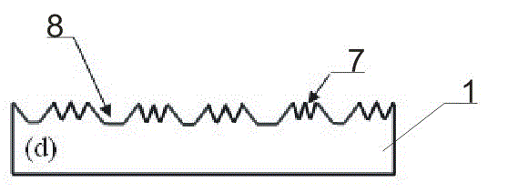
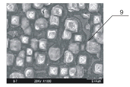
[0079] 3. Finally, put the annealed Cu / Cu-Zr / Si(100) composite film-based system into a mixed corrosion solution composed of 85vol% acetone, 5vol% hydrofluoric acid and 10vol% dilute hydrochloric acid, and perform ultrasonic Shake for 30 minutes, take it out after shaking, wash with absolute ethanol and deionized water, and dry with a hair dryer to obtain a V-shaped groove suede structure; Figure 4 shown.


PUM


Abstract

The invention relates to a method for making a V-shaped groove texture surface on the surface of a monocrystalline silicon solar cell. A V-shaped copper-silicon compound epitaxially grows on monocrystalline silicon, the epitaxially-grown V-shaped copper-silicon compound is removed by wet etching, and a low-reflectivity V-shaped groove texture surface structure is obtained on the surface of the monocrystalline silicon. The method comprises the following steps of: 1, sequentially depositing a Cu-Zr film and a Cu film on the monocrystalline silicon (Si) to form a monocrystalline silicon (Si) composite film substrate system; 2, annealing the composite film substrate system, wherein the temperature is between 100 and 800 DEG C, the vacuum degree is superior to 1*10<-3>, and the time is between5 and 10 minutes; 3, placing the annealed composite film into mixed liquid and oscillating for more than 5 minutes by ultrasound; and 4, cleaning by using absolute ethanol and deionized water, and drying to obtain a product. The invention has the advantages that: the obtained V-shaped grooves have regular shapes, the texture efficiency is higher; the structure can effectively reduce light reflection; and the making cost is reduced by 10 to 15 percent, the quality is improved, and the yield is enhanced by 30 percent.

Description

technical field [0001] The invention relates to the preparation technology of monocrystalline silicon solar cells, in particular to a technology for etching texture on the surface of monocrystalline silicon solar cells, that is, a method for preparing V-shaped grooves on the surface of monocrystalline silicon by means of wet etching. Background technique [0002] In recent years, in order to reduce carbon emissions and promote economic health and sustainable development, the development and industrialization of high-efficiency, low-cost monocrystalline silicon solar cells have received great attention from all over the world, and their applications have become increasingly widespread. However, compared with traditional energy sources, the current production cost of monocrystalline silicon solar cells is still slightly higher, which limits their popularization and application in more fields. Obviously, reducing production costs and improving photoelectric conversion efficienc...

Claims


Application Information

Patent Timeline
Patent Type & Authority Patents(China)
IPC IPC(8): H01L31/18C30B33/10
CPCY02P70/50
Inventor 孙浩亮魏明宋忠孝徐可为刘玉亮
Owner HENAN UNIV OF SCI & TECH
Learn More