Micro-fluidic composite chip with symmetric micro-channel structure and integrated non-contact conductivity detection
A conductivity detection and composite chip technology, which is used in measurement devices, material analysis by electromagnetic means, instruments, etc., can solve the problems that the separation conditions cannot be kept consistent, the separation range is small, and cannot be carried out at the same time, so as to achieve rapid electrophoretic separation analysis. , the effect of improving detection sensitivity and improving the degree of integration
- Summary
- Abstract
- Description
- Claims
- Application Information
AI Technical Summary
Problems solved by technology
Method used
Image
Examples
Embodiment 1
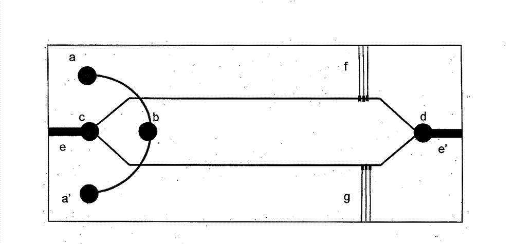
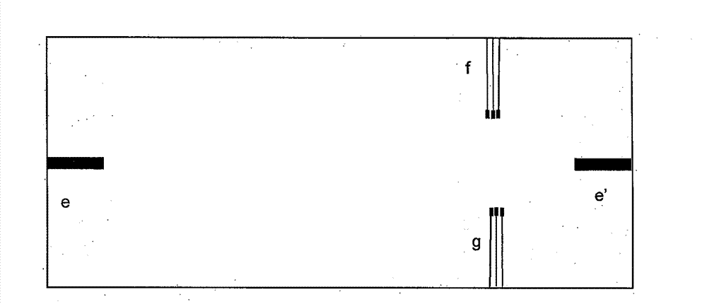
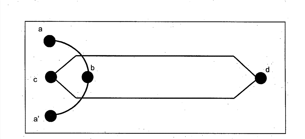
[0023] like Figure 1~4 As shown, a microfluidic composite chip with a symmetrical micropipe structure integrated with non-contact conductivity detection is mainly composed of a glass substrate, a polydimethylsiloxane (PDMS) cover sheet, and a micro control circuit board. The feature is: the microfluidic composite electrophoresis chip is made of a polydimethylsiloxane cover sheet engraved with a symmetrical microchannel structure and a glass substrate deposited with a symmetrical microelectrode at room temperature. The circuit board is connected for conductance detection, and the signals in the two parallel micro-pipes are differentiated, and the separation results are compared under the same conditions.
[0024] The glass substrate has a length of 40000 μm, a width of 18000 μm and a thickness of 600 μm. On the glass substrate, aluminum is sputter-deposited on the glass substrate to form a micro-electrode of a micro-plane thin layer by adopting conventional micro-electro-mech...
Embodiment 2
[0029] A microfluidic composite chip with a symmetrical micropipe structure integrated with non-contact conductance detection, as in Example 1, wherein: the glass substrate has a length of 42000 μm, a width of 19000 μm, and a thickness of 800 μm, and gold is deposited on the glass substrate by sputtering A microelectrode with a microplane thin layer is formed on the chip, and the length of the electrophoretic separation driving microelectrode e, e′ is 4000 μm, the width is 1500 μm, and the thickness is 30 μm. The length of each microelectrode f and g of the online conductance detection microelectrode is 6500 μm, and the width is 650 μm, 30 μm in thickness, 45 μm in distance between two microelectrodes, and 0.4 μm in thickness of the silicon dioxide insulating layer deposited on the surface of conductance detection microelectrodes f and g. The length of the polydimethylsiloxane cover slip is 38000 μm, the width is 16000 μm, and the thickness is 1200 μm. The diameter of each rese...
Embodiment 3
[0031] A microfluidic composite chip with a symmetrical micropipe structure integrated with non-contact conductance detection, as in Example 1, wherein: the glass substrate has a length of 45000 μm, a width of 20000 μm, and a thickness of 1000 μm, and titanium-tungsten alloy is sputter-deposited on A microelectrode with a microplane thin layer is formed on a glass substrate. The length of the electrophoretic separation-driven microelectrode e, e' is 5000 μm, the width is 2000 μm, and the thickness is 50 μm. The width is 700 μm, the thickness is 50 μm, the distance between two microelectrodes is 50 μm, and the thickness of the silicon nitride insulating layer deposited on the surface of conductance detection microelectrodes f and g is 0.5 μm. The length of the polydimethylsiloxane cover sheet is 40000 μm, the width is 18000 μm, and the thickness is 1500 μm. The diameter of each reservoir is 3000 μm and the depth is 1500 μm. The distance between the centers of the two sample pool...
PUM
| Property | Measurement | Unit |
|---|---|---|
| length | aaaaa | aaaaa |
| length | aaaaa | aaaaa |
| length | aaaaa | aaaaa |
Abstract
Description
Claims
Application Information
 - Generate Ideas
- Intellectual Property
- Life Sciences
- Materials
- Tech Scout
- Unparalleled Data Quality
- Higher Quality Content
- 60% Fewer Hallucinations
Browse by: Latest US Patents, China's latest patents, Technical Efficacy Thesaurus, Application Domain, Technology Topic, Popular Technical Reports.
© 2025 PatSnap. All rights reserved.Legal|Privacy policy|Modern Slavery Act Transparency Statement|Sitemap|About US| Contact US: help@patsnap.com


