Flexible substrate, flexible AMOLED (Active Matrix/Organic Light Emitting Diode) and flexible PMOLED (Passive Matrix/Organic Light Emitting Diode)
A flexible substrate and substrate technology, applied in the direction of circuit substrate materials, electrical components, circuits, etc., can solve the problems of OLED failure, high permeability, poor temperature stability, etc., and achieve low water and oxygen transmission rate, strong adhesion performance, good transparency effect
- Summary
- Abstract
- Description
- Claims
- Application Information
AI Technical Summary
Problems solved by technology
Method used
Image
Examples
Embodiment 1
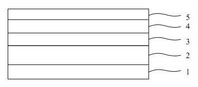
[0025] A flexible substrate, comprising a polyimide substrate, an inorganic layer is arranged on the polyimide substrate, at least one polyimide layer is arranged on the inorganic layer, and each layer of the polyimide An inorganic layer is also provided on the imide layer.
[0026] Such as figure 1 As shown, in a preferred embodiment, the bottom of the polyimide substrate is also provided with an inorganic protective layer, the material of the inorganic layer is at least one of silicon dioxide, silicon oxynitride, aluminum oxide and aluminum nitride, inorganic The material of the protective layer is at least one of silicon dioxide, silicon oxynitride, aluminum oxide and aluminum nitride. In this embodiment, the material of each inorganic layer is the same, and the material of the inorganic protective layer is the same as that of the inorganic layer. It is also the same (in practice, different materials can be used for each inorganic layer, and the material of the inorganic p...
Embodiment 2
[0034] The difference with Embodiment 1 is that: using SiO 2 As the material of the inorganic protective layer and each inorganic layer, SiO is grown on the PI substrate 2 by magnetron sputtering, electron beam evaporation, and PECVD. 2 Film, the layer of film has compressive stress. Process parameters when using PECVD technology: PI substrate temperature is 25°C-300°C, RF power is 20-200W, background vacuum is 5×10 -3 Pa, RF power frequency 13.56MHz, working gas is 10% silane SiH 4 and 99.999% of N 2 O, N 2 O:SiH 4 The flow ratio is 1:1-2:1.
Embodiment 3
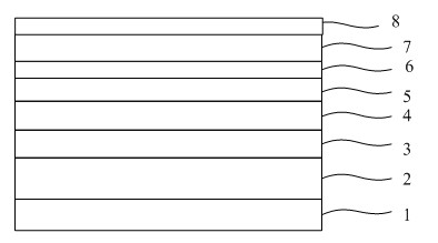
[0036] Such as figure 2 As shown, a flexible passively driven organic light-emitting device includes a flexible substrate and a passive organic light-emitting device disposed on the flexible substrate, wherein the flexible substrate is the flexible substrate in Embodiment 1 or Embodiment 2.
[0037] The passively driven organic light emitting device sequentially comprises an anode transparent conductive layer 6 , an organic functional layer 7 on the anode transparent conductive layer 6 , and an OLED cathode 8 on the organic functional layer 7 .
[0038] The anode transparent conductive layer 6 of OLED is formed on the inorganic layer 5 in the flexible substrate, and it can adopt ITO (In 2 o 3 :Sn), SnO 2 :F, SnO 2 : Sb, IZO (ZnO:In), AZO (ZnO:Al), etc., preferably an amorphous transparent conductive layer, such as ZnO:Ga.
[0039] The radio frequency magnetron sputtering apparatus is carried out at room temperature, the sputtering frequency is 13.56MNHz, and the background ...
PUM
| Property | Measurement | Unit |
|---|---|---|
| Thickness | aaaaa | aaaaa |
| Thickness | aaaaa | aaaaa |
| Thickness | aaaaa | aaaaa |
Abstract
Description
Claims
Application Information
 - R&D Engineer
- R&D Manager
- IP Professional
- Industry Leading Data Capabilities
- Powerful AI technology
- Patent DNA Extraction
Browse by: Latest US Patents, China's latest patents, Technical Efficacy Thesaurus, Application Domain, Technology Topic, Popular Technical Reports.
© 2024 PatSnap. All rights reserved.Legal|Privacy policy|Modern Slavery Act Transparency Statement|Sitemap|About US| Contact US: help@patsnap.com


