Preparation method of germanium substrate on insulator

A germanium substrate and substrate technology, which is applied in the field of new semiconductor materials and devices, can solve the problems of poor quality of the back interface of GeOI substrate and the like

Inactive Publication Date: 2011-10-19
PEKING UNIV
View PDF6 Cites 3 Cited by
  • Summary
  • Abstract
  • Description
  • Claims
  • Application Information

AI Technical Summary

Problems solved by technology

[0004] In view of the poor quality of the back interface of the GeOI substrate

Method used


Image

  • Preparation method of germanium substrate on insulator
  • Preparation method of germanium substrate on insulator
  • Preparation method of germanium substrate on insulator

Examples


Embodiment Construction

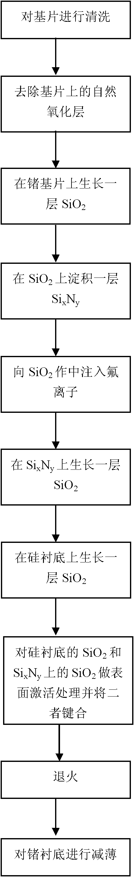
[0031] specific implementation plan

[0032] Step 1. Select a semiconductor germanium substrate and a silicon substrate, as shown in Figure 2(a). Clean the germanium substrate and the silicon substrate respectively. First, the germanium substrate is organically cleaned, soaked and cleaned with acetone and ethanol in turn, and then rinsed with DI water to remove oil and organic pollutants on the germanium substrate. Then wash with hydrochloric acid, heat and boil in dilute hydrochloric acid, and then rinse with DI water to remove inorganic pollutants, metal particles, etc.; first use No. 1 cleaning solution (NH 4 OH:H 2 o 2 :H 2 (0=1:1:5˜1:2:7) to clean the silicon substrate, and then clean it with deionized water to remove particles and organic substances on the substrate. Then use No. 2 cleaning solution (HCl: H 2 o 2 :H 2 O=1:1:6~1:2:8) cleaning, and then cleaning with deionized water to remove metal contamination on the substrate;

[0033] Step 2. Removing the natu...


PUM


Abstract

The invention provides a preparation method of a GeOI substrate on an insulator, belonging to the field of novel semiconductor material. The preparation method of a GeOI substrate comprises the following steps: while preparing the GeOI substrate, SiO2 with injected fluorine ions is adopted to realize the passivating treatment of germanium and buried oxygen layer interface; therefore, the density of interface state is reduced, and the preparation method is beneficial to improving the back interface quality of GeOI substrate. Moreover, the dielectric constant of the buried oxygen layer is decreased, and the preparation method is beneficial to inhibiting the short channel effect of GeOI MOSFET (Metal-Oxide-Semiconductor Field-Effect Transistor) device.

Description

technical field [0001] The invention belongs to the field of novel semiconductor material devices, and in particular relates to a germanium-on-insulator (GeOI) substrate preparation technology. Background technique [0002] Integrated circuit technology has followed Moore's law for more than 40 years. The method of increasing the working speed by reducing the geometric size of the device is facing the double test of the physical limit of the transistor size and the technical limit. In order to continue to improve the operating speed of devices, new materials and device structures need to be adopted. Due to its high carrier mobility (at room temperature, the electron mobility is 2.4 times that of silicon, and the hole mobility is 4 times that of silicon), it is considered to be a very potential candidate material for future CMOS devices. Therefore, Ge-based devices have become one of the international research hotspots in recent years. In addition, the "On Insulator" struct...

Claims


Application Information

Patent Timeline
IPC IPC(8): H01L21/762H01L21/84
Inventor 黄如林猛安霞张兴
Owner PEKING UNIV
Why Eureka
Try Eureka