Piezoelectric film, piezoelectric device, liquid ejection apparatus, and method of producing piezoelectric film

A piezoelectric film and liquid technology, applied in the field of preparing the piezoelectric film, can solve problems such as durability decline, cracks, PZT film cracks, etc., and achieve the effects of improving driving durability, preventing formation of defects, and improving driving durability.

Active Publication Date: 2011-09-21
FUJIFILM CORP
View PDF7 Cites 4 Cited by
  • Summary
  • Abstract
  • Description
  • Claims
  • Application Information

AI Technical Summary

Problems solved by technology

However, using the sol-gel method to prepare PZT films with a thickness of at least 2 μm may cause cracks in the PZT films due to the thermal stress generated by repeated coating and sintering steps
Therefore, it is difficult to prepare PZT thin films at least 2 μm thick using the sol-gel method
In addition, when the PZT thin film is prepared using the sol-gel method, horizontal stripes are caused every time the crystallization is performed by sintering, and when the piezoelectric crystal repeatedly performs functions related to the piezoelectric effect, the stripe defects cause cracks, resulting in durable sex decline

Method used


Image

  • Piezoelectric film, piezoelectric device, liquid ejection apparatus, and method of producing piezoelectric film
  • Piezoelectric film, piezoelectric device, liquid ejection apparatus, and method of producing piezoelectric film
  • Piezoelectric film, piezoelectric device, liquid ejection apparatus, and method of producing piezoelectric film

Examples


Embodiment 1

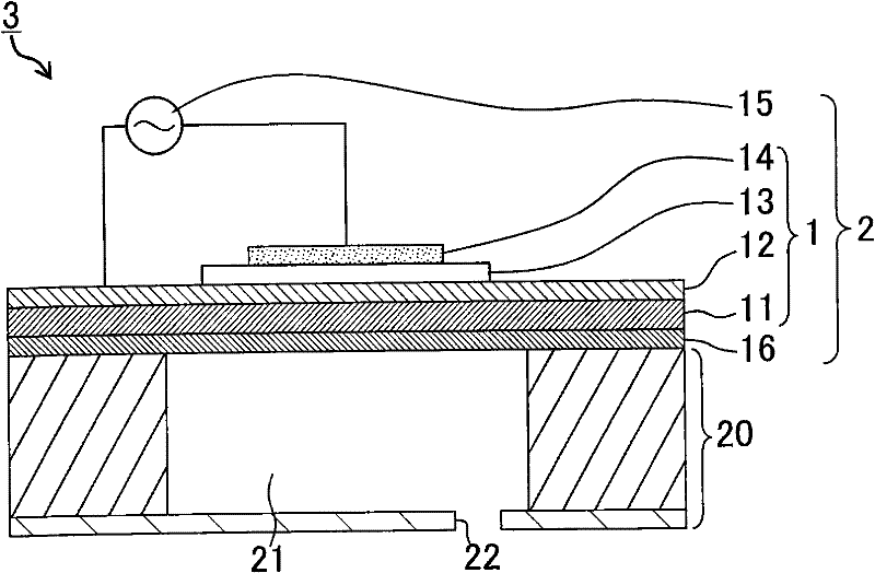
[0131] Using a sputtering method at a substrate temperature of 350° C., a Ti film with a thickness of 30 nm and an Ir film with a thickness of 150 nm were sequentially formed on an SOI substrate to obtain a lower electrode. A Nb-doped PZT piezoelectric thin film with a thickness of 4 μm was formed on this lower electrode. Formation of this thin film was performed under the following conditions.

[0132] >

[0133] Film forming device: RF sputtering device

[0134] Target: Pb 1.3 ((Zr 0.52 Ti 0.48 ) 0.88 Nb 0.12 ) O 3 Sintered body (amount of Nb occupying the B site: 12 mol%)

[0135] Substrate temperature: 475°C

[0136] Target-substrate (T-S) distance: 60mm

[0137] Film forming pressure: 0.30Pa

[0138] Film-forming gas: Ar / O 2 =97.5 / 2.5 (molar ratio)

[0139] Substrate potential Vsubstrate = -12V

[0140] After the start of film formation, the substrate potential V 基板 Set at +25V for 5 minutes to provide the perovskite layer as the initial layer.

[0141] Af...

Embodiment 2-6

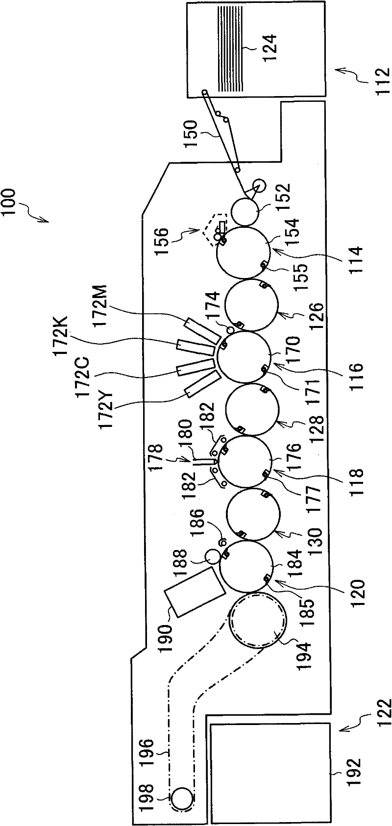
[0151] Using the same method as Example 1 in Figure 5 A piezoelectric thin film and an ink jet recording head were prepared under the conditions described, and the resulting piezoelectric thin film and ink jet recording head were evaluated.


PUM

PropertyMeasurementUnit
thicknessaaaaaaaaaa
piezoelectric charge coefficientaaaaaaaaaa
thicknessaaaaaaaaaa

Abstract

The invention relates to a piezoelectric film, a piezoelectric device, a liquid ejection apparatus, and a method of producing piezoelectric film. The piezoelectric film is formed on a surface of a substrate by a vapor deposition process without generating grain boundaries which are substantially parallel to the surface of the substrate and are caused by lamination. A normal of a (100) plane of each of crystals constituting the piezoelectric film is inclined from a normal of the surface of the substrate by an angle of not smaller than 6 DEG and not larger than 36 DEG .

Description

technical field [0001] The present invention relates to a piezoelectric thin film, a piezoelectric device, a liquid ejecting apparatus, and a method for producing a piezoelectric thin film, and more particularly, to a piezoelectric thin film having improved durability in continuous driving, and a piezoelectric device including the piezoelectric thin film , a liquid ejecting device including the piezoelectric device, and a method of manufacturing the piezoelectric thin film. Background technique [0002] It is known to obtain a piezoelectric device by combining a piezoelectric thin film having a piezoelectric property of being displaced by application of a driving voltage applied to the piezoelectric thin film through the electrodes. [0003] For example, Japanese Patent Application Laid-Open No. 11-307833 describes a piezoelectric device in which the (100) orientation in a crystal in which a piezoelectric thin film is formed is inclined by 5° to 20°. Tilting the (100) orien...

Claims


Application Information

Patent Timeline
Patent Type & Authority Applications(China)
IPC IPC(8): H01L21/20H01L41/187H01L41/09H01L41/24B41J2/045B41J2/055B41J2/135B41J2/14B41J2/16C23C14/08C23C16/40H01L41/18
CPCH01L41/316H01L41/0973B41J2/1646H01L41/18H01L41/0805H01L41/1876B41J2/1642B41J2/1612B41J2/14233B41J2/1645H10N30/1051H10N30/2047H10N30/8554H10N30/076
Inventor 直野崇幸
Owner FUJIFILM CORP
Why Eureka
Try Eureka