Preparation method of patterned substrate
A patterned substrate and graphics technology, applied in semiconductor/solid-state device manufacturing, electrical components, circuits, etc., can solve problems such as inapplicability, achieve the effect of improving crystal quality, improving crystal growth quality, and reducing dislocation density
- Summary
- Abstract
- Description
- Claims
- Application Information
AI Technical Summary
Problems solved by technology
Method used
Image
Examples
preparation example Construction
[0065] The preparation method involved in the present invention is as follows:
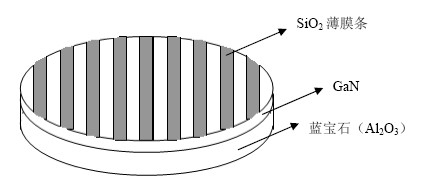
[0066] Firstly, a certain thickness of single crystal heterogeneous material, such as SiO, is grown on a sapphire substrate using PECVD, MOCVD, CVD or magnetron sputtering techniques well known to those skilled in the art. 2 , Si 3 N 4 , SiC, Si, ZnO, GaAs series materials and other materials. The thickness can be from 100 nanometers to 3 micrometers, with 500 nanometers to 1.8 micrometers being preferred.
[0067] Secondly, using the glue spinning technology well known to those skilled in the art, the single crystal heterogeneous material (such as SiO 2 , Si 3 N 4 , SiC, Si, ZnO, GaAs series materials and other materials) uniformly coat photoresist on the sapphire substrate (this photoresist can be positive or negative, as long as the corresponding photoresist can be used to obtain the same pattern Yes), and the photoresist is evenly spun by the spun glue technology. The thickness of the photoresist i...
Embodiment 1
[0078] Complete SiO 2 To prepare the patterned substrate with periodic patterns, see attached Picture 9 :
[0079] Step 1. Select a 2-inch sapphire substrate 3 with a thickness of 430 microns; attached Picture 9 The first step is a 430-micron thick 2-inch sapphire substrate;
[0080] Step 2. Using PECVD technology to grow SiO with a thickness of 1.5 microns on the sapphire substrate 3 2 Film 2, attached Picture 9 The second step is to grow 1.5 microns thick SiO 2 The thin film 2 is a 430 micrometer thick 2-inch sapphire substrate 3;
[0081] 1~1.5 microns thick SiO 2 Thin film 2,2-430 micron thick sapphire substrate;
[0082] Step 3. Use the spinner to prepare the substrate SiO after step 2 2 The surface is evenly coated with 1.5 micron thick photoresist 1; attached Picture 9 The third step is SiO coated with 1.5 micron photoresist 1 2 / Sapphire substrate;
[0083] 1~1.5μm photoresist 1, 2~1.5μm thick SiO 2 Thin film 2,3~430 microns thick sapphire 3;
[0084] Step 4. SiO coated with...
Embodiment 2
[0090] SiO 2 Patterned substrate layered with sapphire to form periodic patterns
[0091] Step 1. Select a 2-inch sapphire substrate 3 with a thickness of 430 microns;
[0092] Step 2. Using PECVD technology to grow SiO with a thickness of 1.5 microns on the sapphire substrate 3 2 Film 2;
[0093] 1~1.5 microns thick SiO 2 Thin film 2, 2~430 microns thick sapphire substrate 3;
[0094] Step 3. Use the spinner to prepare the substrate SiO after step 2 2 The surface is evenly coated with 1.5 micron thick photoresist 1 to become SiO after coating 1.5 micron photoresist 2 / Sapphire substrate;
[0095] 1~1.5μm photoresist 1, 2~1.5μm thick SiO 2 , 3~430 microns thick sapphire substrate 3;
[0096] Step 4. SiO coated with 1.5 micron photoresist 1 2 / The sapphire substrate is exposed by a step exposure machine and developed to form a cylindrical pattern with a surface period of 3 microns and a cylindrical diameter of 2 microns, a periodic cylindrical photoresist pattern with a period of 3 micron...
PUM
| Property | Measurement | Unit |
|---|---|---|
| Thickness | aaaaa | aaaaa |
| Bottom diameter | aaaaa | aaaaa |
| Height | aaaaa | aaaaa |
Abstract
Description
Claims
Application Information
 - Generate Ideas
- Intellectual Property
- Life Sciences
- Materials
- Tech Scout
- Unparalleled Data Quality
- Higher Quality Content
- 60% Fewer Hallucinations
Browse by: Latest US Patents, China's latest patents, Technical Efficacy Thesaurus, Application Domain, Technology Topic, Popular Technical Reports.
© 2025 PatSnap. All rights reserved.Legal|Privacy policy|Modern Slavery Act Transparency Statement|Sitemap|About US| Contact US: help@patsnap.com


