
Complementary metal-oxide-semiconductor (CMOS) ring oscillator based on mixed crystal orientation silicon on insulator (SOI) technology and manufacturing method thereof

A ring oscillator and mixed crystal orientation technology are applied in the CMOS ring oscillator and its preparation, and the CMOS ring oscillator based on the mixed crystal orientation SOI process and its preparation field can solve the problems of reducing the circuit integration density and the like.

Inactive Publication Date: 2011-06-15
SHANGHAI INST OF MICROSYSTEM & INFORMATION TECH CHINESE ACAD OF SCI +1
View PDF6 Cites 13 Cited by
  • Summary
  • Abstract
  • Description
  • Claims
  • Application Information

AI Technical Summary

Problems solved by technology

That is, designing to increase speed will reduce the integration density of the circuit

Method used


Image

  • Complementary metal-oxide-semiconductor (CMOS) ring oscillator based on mixed crystal orientation silicon on insulator (SOI) technology and manufacturing method thereof
  • Complementary metal-oxide-semiconductor (CMOS) ring oscillator based on mixed crystal orientation silicon on insulator (SOI) technology and manufacturing method thereof
  • Complementary metal-oxide-semiconductor (CMOS) ring oscillator based on mixed crystal orientation silicon on insulator (SOI) technology and manufacturing method thereof

Examples


Embodiment Construction

[0038] The device structure of the present invention will be further described below in conjunction with the accompanying drawings, which are not drawn to scale for the convenience of illustration.

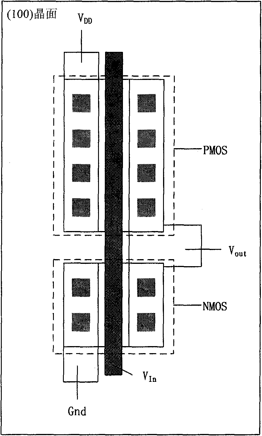
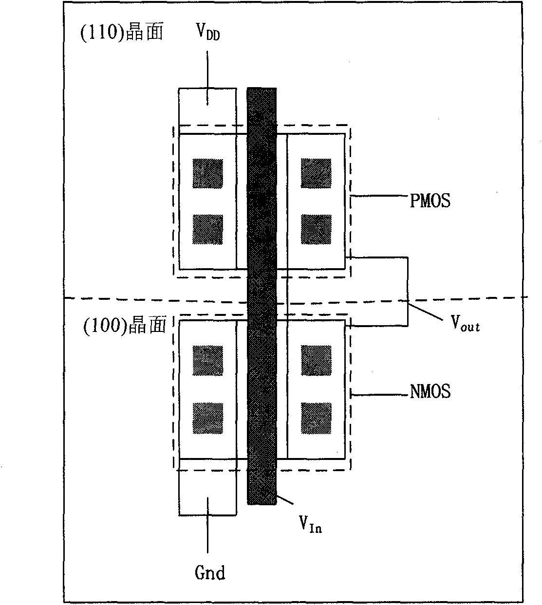
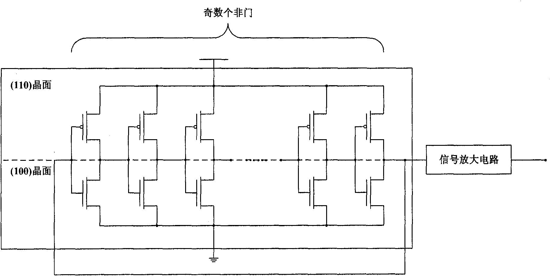
[0039] This embodiment provides a CMOS ring oscillator based on a mixed crystal orientation SOI process, which includes: an SOI substrate and a CMOS device fabricated on the SOI substrate. The CMOS devices include: NMOS devices and PMOS devices. Wherein, the channel of the NMOS device adopts (100) crystal plane silicon, and the channel of the PMOS device adopts (110) crystal plane silicon.

[0040] Since the (110) crystal plane PMOS carrier hole mobility is much higher than that of the traditional (100) crystal plane, depending on the epitaxial quality of the (110) crystal plane, the hole mobility in the (110) crystal plane is the same as that of the (100) crystal plane. 1.5 to 3 times of that, therefore, the channel adopts the PMOS device of (110) crystal plane, can reduce the c...


PUM


Abstract

The invention discloses a complementary metal-oxide-semiconductor (CMOS) ring oscillator based on a mixed crystal orientation silicon on insulator (SOI) technology and a manufacturing method thereof. The oscillator comprises an SOI substrate and a CMOS device which is manufactured on the SOI substrate. The CMOS device comprises an N-channel metal-oxide-semiconductor (NMOS) device and a P-channel metal-oxide-semiconductor (PMOS) device; a channel of the NMOS device is made of a crystal face silicon material (100); and a channel of the PMOS device is made of crystal face silicon material (110). The CMOS device is provided with window epitaxial substrate silicon on a mixed crystal orientation SOI substrate, so that the NMOS device and the PMOS device are formed on the top silicon of the crystal face (100) and an epitaxial silicon layer (110) respectively. According to the invention, the width of a CMOS transistor in the CMOS ring oscillator can be reduced, the integration density is enhanced, the transmission delay time of a NOT gate is reduced, and the oscillation frequency is increased.

Description

technical field [0001] The invention relates to a CMOS ring oscillator and a preparation method, in particular to a CMOS ring oscillator based on a mixed crystal orientation SOI process and a preparation method, and belongs to the technical field of semiconductor manufacturing. Background technique [0002] A phase locked loop (PLL, Phase Lock Loop) is an important unit in a radio frequency (RF, Radio Frequency) circuit, which is used to generate a time reference, and its performance determines the performance of the entire system. Voltage Controlled Oscillator (VCO, Voltage Controlled Oscillator) is the core module in the phase-locked loop circuit, which means that the oscillation frequency is controlled by the input DC signal voltage. There are three main types: [0003] 1. A relaxation oscillator that uses capacitor charging and discharging; [0004] 2. A feedback oscillator that feeds the output signal back to the input for oscillation; [0005] 3. A delay oscillator u...

Claims


Application Information

Patent Timeline
IPC IPC(8): H03K3/02H01L27/12H01L29/04H01L29/78H01L21/84
Inventor 黄晓橹伍青青魏星陈静张苗王曦
Owner SHANGHAI INST OF MICROSYSTEM & INFORMATION TECH CHINESE ACAD OF SCI
Learn More