Heat-type wind-speed and wind-direction sensor with heat insulation structure and preparation method thereof
A technology of wind speed, wind direction, and thermal isolation, which is applied in semiconductor/solid-state device manufacturing, using thermal variables to measure fluid velocity, instruments, etc. It can solve the problems of reducing the output sensitive signal amplitude, increasing the sensor, and unstable performance.
- Summary
- Abstract
- Description
- Claims
- Application Information
AI Technical Summary
Problems solved by technology
Method used
Image
Examples
Embodiment 1
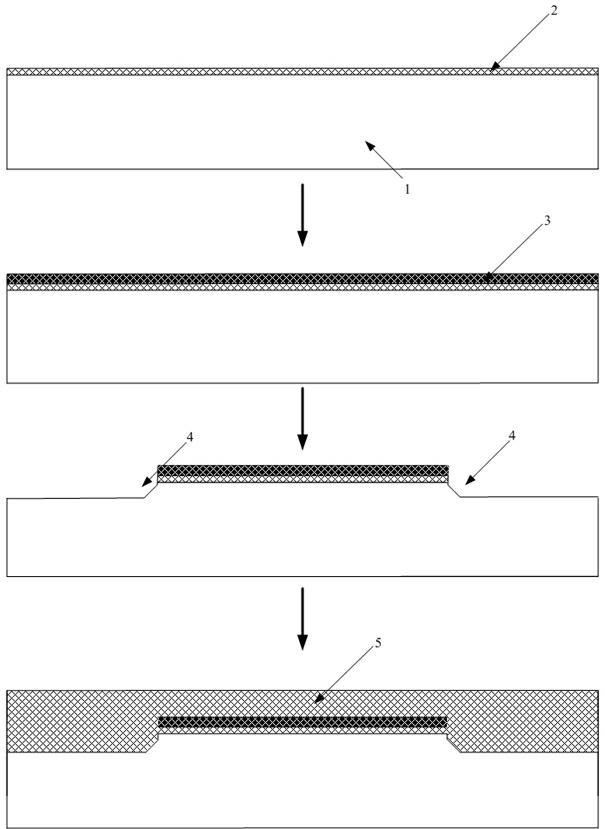
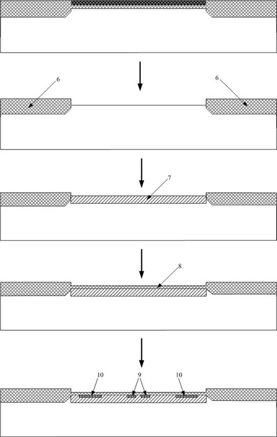
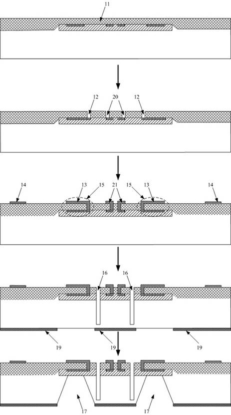
[0045] The manufacturing process of a thermal wind speed and direction sensor with thermal isolation structure is as follows:
[0046] The first step, the preparation of the silicon chip, see Figure 1 to Figure 3
[0047] Step 1, thermally growing a first thermal oxide layer 2 on the surface of the silicon chip 1;
[0048] Step 2, chemical vapor deposition of a silicon nitride layer 3 on the first thermal oxide layer 1;
[0049] Step 3, using RIE technology to etch the silicon chip 1 to define the active region 4;
[0050] Step 4, chemical vapor deposition of the second oxide layer 5;
[0051] Step 5, using CMP technology to polish the silicon chip 1;
[0052] Step 6, removing the silicon nitride layer 3 by wet etching, and preparing the field oxide layer 6;
[0053] Step 7, P ion implantation to prepare N well 7;
[0054] Step 8, thermally growing the gate oxide layer 8;
[0055] Step 9, B ion implantation, preparing the heating resistor 9 and one end 10 of the temperat...
Embodiment 2
[0069] A thermal wind speed and direction sensor with a thermal isolation structure, comprising a silicon chip 1 and a ceramic substrate 20, the silicon chip 1 is located above the ceramic substrate 20, four heating elements 9 and 4 heat-sensing temperature-measuring elements 15, characterized in that a heat-insulating groove 16 is arranged between the heating element 9 and the heat-sensing temperature-measuring element 15, below the heat-sensing temperature-measuring element 15 on the back side of the silicon chip 1 A heat insulation cavity 17 is provided, and a gold layer 18 on ceramics and a gold layer 19 on silicon are provided between the silicon chip 1 and the ceramic substrate 20, and the gold layer 18 on ceramics and the gold layer 19 on silicon are connected through a gold-gold bonding process, It is used for thermal connection between the silicon chip 1 and the ceramic substrate 20 .
PUM
 Abstract
Description
Claims
Application Information
 - R&D
- Intellectual Property
- Life Sciences
- Materials
- Tech Scout
- Unparalleled Data Quality
- Higher Quality Content
- 60% Fewer Hallucinations
Browse by: Latest US Patents, China's latest patents, Technical Efficacy Thesaurus, Application Domain, Technology Topic, Popular Technical Reports.
© 2025 PatSnap. All rights reserved.Legal|Privacy policy|Modern Slavery Act Transparency Statement|Sitemap|About US| Contact US: help@patsnap.com


