Conductive particle, anisotropic conductive film, joined body, and connecting method
A conductive particle, anisotropic technology, used in conductive connections, electrical component connections, conductive materials dispersed in non-conductive inorganic materials, etc. problems, to achieve the effects of suppressing stress, fully conducting reliability, and improving spreadability
- Summary
- Abstract
- Description
- Claims
- Application Information
AI Technical Summary
Problems solved by technology
Method used
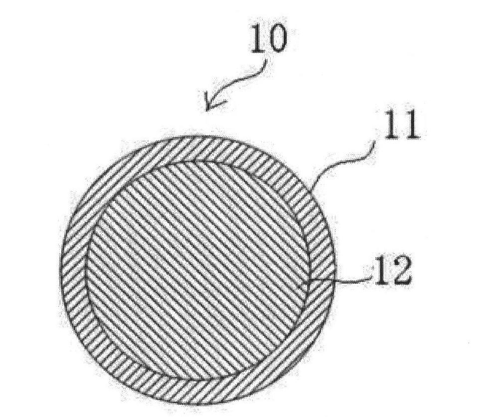
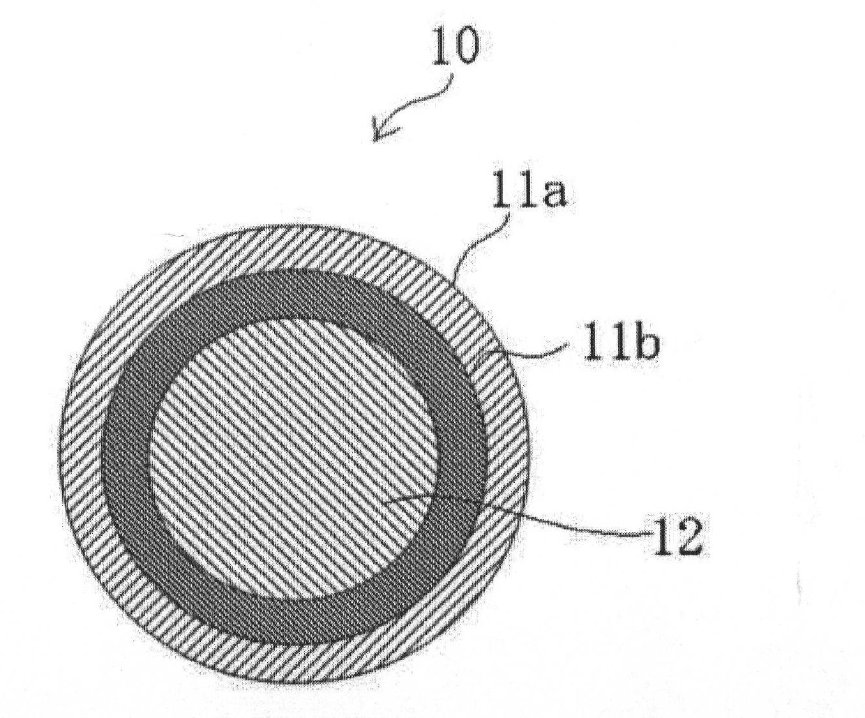
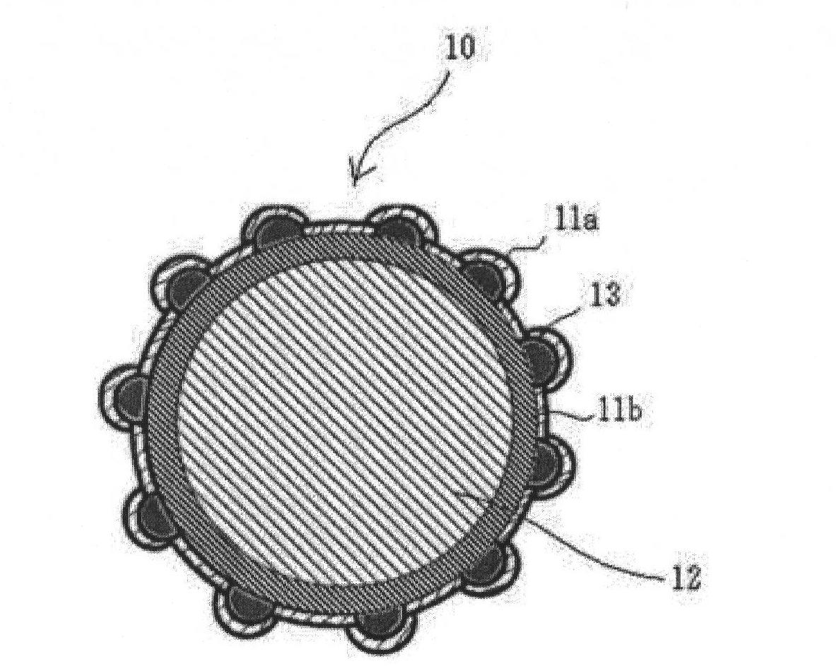
Image

Examples
Embodiment 1
[0144] A palladium catalyst (manufactured by Muromachi Technos, trade name: MK-2605) was loaded on the surface of the resin particles produced in Comparative Example 1, and the resin particles were activated with an accelerator (manufactured by Muromachi Technos, trade name: MK-370); The latter resin particles are added to a mixed solution of palladium chloride, nickel chloride, ethylenediamine, thiodiacetic acid, and sodium hypophosphite adjusted to pH 8 with ammonia at a water bath temperature of 60°C to make the outermost Conductive particles A3 coated with a nickel-palladium alloy (the outermost layer is a nickel-palladium alloy layer); then, as in Comparative Example 1, evaluation of conductive particles A3, preparation of anisotropic conductive film, and IZO wiring The preparation of assembly A3, the preparation of ITO wiring assembly A3, and the measurement of the connection resistance of assembly A3. The results are shown in Table 1 and Table 2.
Embodiment 2
[0146] In Comparative Example 1, the following nickel-palladium alloy plating was used instead of gold plating, except that the preparation of conductive particles A4, the evaluation of conductive particles A4, and the evaluation of the anisotropic conductive film were performed in the same manner as in Comparative Example 1. Preparation, preparation of IZO wiring assembly A4, preparation of ITO wiring assembly A4, and measurement of connection resistance of assembly A4. The results are shown in Table 1 and Table 2.
[0147]
[0148] Add conductive particles coated with nickel to the mixed solution of palladium chloride, nickel chloride, ethylenediamine, thiodiacetic acid and sodium hypophosphite. After mixing, adjust the pH to 8 with ammonia water, and the temperature of the water bath is 60 At °C, conductive particles A4 in which the outermost layer is plated with a nickel-palladium alloy (the outermost layer is a nickel-palladium alloy layer) are prepared.
Embodiment 3
[0150] After the resin particles produced in Comparative Example 1 were dispersed in deionized water for 3 minutes, nickel paste (100 nm) was added and stirred to obtain substrate particles with nickel paste attached. Then, the same treatment as the pre-process and post-process of the electroless plating of nickel plating of Comparative Example 1 was performed to prepare conductive particles with nickel protrusions. Then, the nickel-palladium alloy plating in Example 2 was performed to prepare conductive particles A5. Then, in the same manner as in Comparative Example 1, the evaluation of conductive particles A5, the preparation of anisotropic conductive film, and the evaluation of IZO wiring assembly A5 were performed. Preparation, preparation of ITO wiring assembly A5, and measurement of connection resistance of assembly A5. The results are shown in Table 1 and Table 2.
PUM
| Property | Measurement | Unit |
|---|---|---|
| glass transition temperature | aaaaa | aaaaa |
| coating thickness | aaaaa | aaaaa |
| particle diameter | aaaaa | aaaaa |
Abstract
Description
Claims
Application Information
 - R&D
- Intellectual Property
- Life Sciences
- Materials
- Tech Scout
- Unparalleled Data Quality
- Higher Quality Content
- 60% Fewer Hallucinations
Browse by: Latest US Patents, China's latest patents, Technical Efficacy Thesaurus, Application Domain, Technology Topic, Popular Technical Reports.
© 2025 PatSnap. All rights reserved.Legal|Privacy policy|Modern Slavery Act Transparency Statement|Sitemap|About US| Contact US: help@patsnap.com