
Metal oxide semiconductor field effect transistor and manufacturing method thereof

An oxide semiconductor and field effect transistor technology, which is applied in the field of improving metal oxide semiconductor field effect transistors and their manufacturing, and can solve the problems of high thermal stress, increased connection leakage rate, and decreased device performance.

Inactive Publication Date: 2011-04-20
SEMICON MFG INT (SHANGHAI) CORP
View PDF0 Cites 8 Cited by
  • Summary
  • Abstract
  • Description
  • Claims
  • Application Information

AI Technical Summary

Problems solved by technology

However, MSA will cause high thermal stress inside the device, and the SiGe in the source / drain will experience stress relaxation in a high-temperature environment. Under the combined effect of the above factors, SiGe may undergo relative displacement and cause stacking (Overlay, OVL) problems, defect diffusion problems, etc., which lead to device performance degradation
A worse case occurs when the defect diffuses from the SiGe layer deep into the silicon substrate, resulting in a substantial increase in the connection leakage rate

Method used

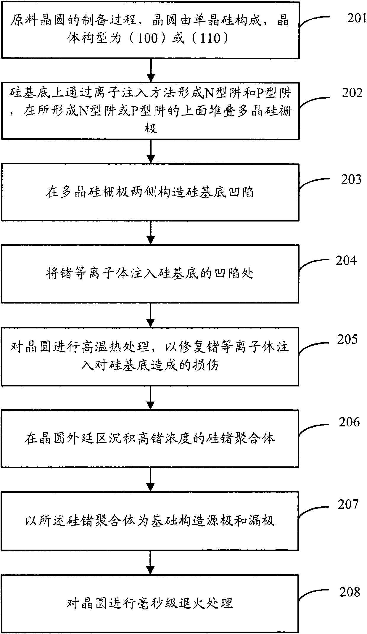

Image

  • Metal oxide semiconductor field effect transistor and manufacturing method thereof
  • Metal oxide semiconductor field effect transistor and manufacturing method thereof
  • Metal oxide semiconductor field effect transistor and manufacturing method thereof

Examples


Embodiment Construction

[0030] The root cause of SiGe stress relaxation is the difference in lattice constants between SiGe and Si. The lattice constant of Ge is 5.6 angstroms, the lattice constant of Si is 5.4 angstroms, and the range of the lattice constant of epitaxial SiGe is between 5.4 angstroms and 5.6 angstroms. The higher the Ge concentration, the greater the difference between the lattice constant of SiGe and the lattice constant of Si, and the greater the difference, the greater the stress on the interface between SiGe and Si, and the greater the stress will be. Will cause SiGe stress relaxation.

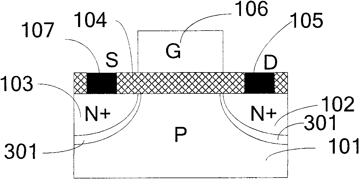
[0031] Aiming at the root cause of SiGe stress relaxation, the solution adopted by the present invention is to form a buffer layer between SiGe and the silicon substrate. The lattice constant of the buffer layer is close to the lattice constant of Si of 5.4 angstroms on the side close to the Si substrate. The side close to the SiGe layer is close to the lattice constant of SiGe. The internal latt...


PUM

PropertyMeasurementUnit
lattice constantaaaaaaaaaa

Abstract

The invention discloses a metal oxide semiconductor field effect transistor (MOSFET), comprising a silicon substrate and a source and a drain which are formed by doped silicon-germanium polymers, wherein buffer layers formed by injection of germanium plasmas are respectively arranged between the silicon substrate and the source as well as between the silicon substrate and the drain. The invention also discloses a manufacturing method of the MOSFET. The invention can effectively avoid the defects caused by stress relaxation of the silicon-germanium polymer layers.

Description

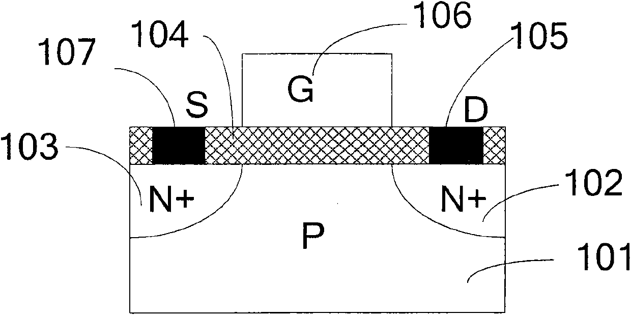
Technical field [0001] The invention relates to the technical field of semiconductor integrated current manufacturing, in particular to an improved metal oxide semiconductor field effect transistor and a manufacturing method thereof. Background technique [0002] Metal-Oxide-Semiconductor Field-Effect Transistor (MOSFET) is a field effect transistor that can be widely used in analog and digital circuits. -effect transistor). MOSFETs can be divided into n-type and p-type MOSFETs according to the polarity of their "channels". They are usually called NMOSFET and PMOSFET. Other abbreviations include NMOS FET, PMOS FET, nMOSFET, pMOSFET, etc. [0003] figure 1 It is a cross-sectional view of a typical NMOSFET. Using P-type silicon semiconductor material as the silicon substrate 101, two shallow trenches (STI) are etched on the silicon substrate 101, and n-type material is deposited in the shallow trenches to form two n-type regions 102 and 103; A silicon oxide film is deposited on th...

Claims


Application Information

Patent Timeline
Patent Type & Authority Applications(China)
IPC IPC(8): H01L29/78H01L29/06H01L27/092H01L21/8238H01L21/265
Inventor 陈勇何永根
Owner SEMICON MFG INT (SHANGHAI) CORP
Learn More