Adhesive sheet for supporting and protecting semiconductor wafer, back grinding method for semiconductor wafer

A technology of semiconductors and adhesive sheets, which is applied in the direction of semiconductor devices, semiconductor/solid-state device manufacturing, adhesive types, etc., and can solve the problems of residual glue, wafer damage, insufficient bonding of adhesives and wafer surfaces, etc. problems, to achieve the effect of preventing residual glue

Inactive Publication Date: 2011-03-30
NITTO DENKO CORP
View PDF4 Cites 7 Cited by
  • Summary
  • Abstract
  • Description
  • Claims
  • Application Information

AI Technical Summary

Problems solved by technology

[0007] Therefore, in the method of using the conventional adhesive sheet, the sheet cannot sufficiently follow the unevenness, and the bonding between the adhesive and the wafer surface is insufficient.
As a result, during wafer processing, peeling of flakes, intrusion of grinding water and foreign matter into the pattern surface, processing errors, dents, chip flying, etc. may occur, and wafer damage may occur.
[0008] In addition, when the adhesive sheet is peeled off from the semiconductor wafer, the adhesive embedded in the unevenness may be broken, and adhesive residue may be generated on the semiconductor wafer side.
In particular, when a relatively soft adhesive is used in order to make the adhesive sheet follow unevenness well, there is a problem that more adhesive residue occurs

Method used


Image

  • Adhesive sheet for supporting and protecting semiconductor wafer, back grinding method for semiconductor wafer
  • Adhesive sheet for supporting and protecting semiconductor wafer, back grinding method for semiconductor wafer
  • Adhesive sheet for supporting and protecting semiconductor wafer, back grinding method for semiconductor wafer

Examples


Embodiment 1

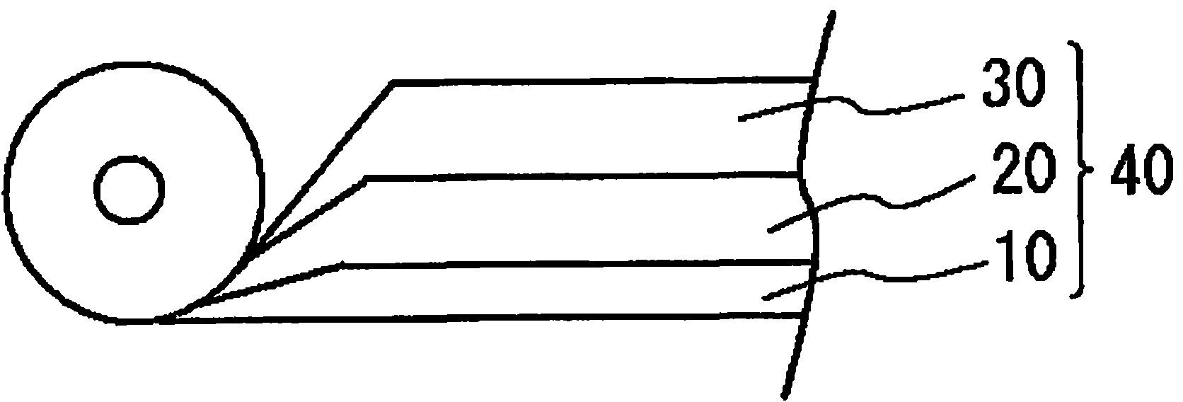
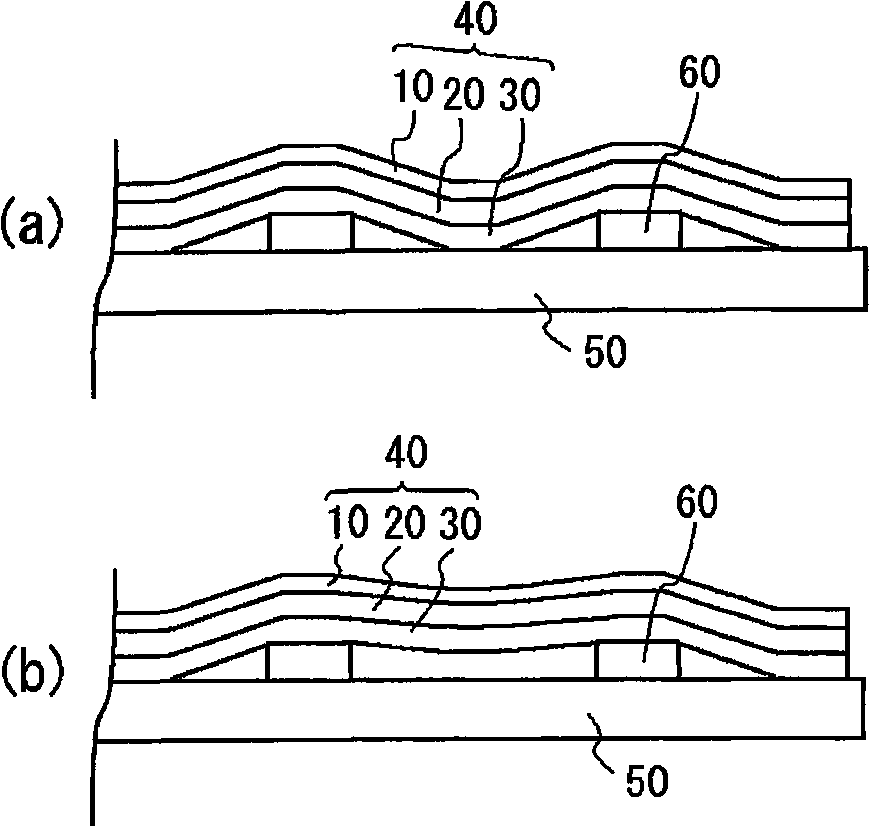
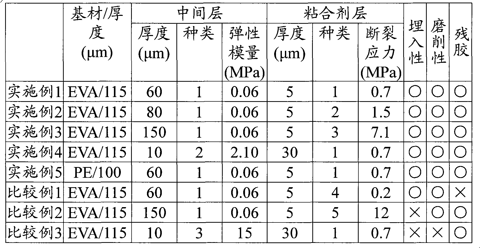
[0186] Such as figure 1 As shown, as the substrate layer 10, an ethylene-vinyl acetate copolymer (EVA) film with a thickness of 115 μm was used, and an intermediate layer 20 (thickness: 60 μm) and an adhesive layer 30 (thickness: 5 μm) were formed thereon.

Embodiment 2~5 and comparative example 1~3

[0188] As the substrate layer, an ethylene-vinyl acetate copolymer (EVA) film with a thickness of 115 μm or a polyethylene (PE) film with a thickness of 100 μm was used.

[0189] According to Example 1, the intermediate layer and the adhesive layer shown in Table 1 were formed on the substrate layer according to the thicknesses in Table 1, respectively.

[0190] Each obtained adhesive sheet was adhered to a silicon wafer, ground, and the adhesive sheet was peeled off, and the following evaluations were performed. Moreover, 25 adhesive sheets of each Example and a comparative example were prepared and evaluated. The results are shown in Table 1.

[0191] paste

[0192] Each adhesive sheet was pasted so that an adhesive layer was disposed on the surface side of an 8-inch silicon wafer on which dummy bump electrodes were formed. Bump electrodes with a height of 50 μm and a diameter of 100 μm were formed on the silicon wafer in a lattice shape with a pitch P of 200 μm, and th...


PUM

PropertyMeasurementUnit
thicknessaaaaaaaaaa
thicknessaaaaaaaaaa
elastic modulusaaaaaaaaaa

Abstract

The invention aims at providing an adhesive sheet for supporting and protecting a semiconductor wafer, and a back grinding method for the semiconductor wafer. The adhesive sheet can effectively prevent adhesive residue caused by concave-convex parts in a forming surface of circuit patterns and the like of the semiconductor wafer in recent years. The adhesive sheet for supporting and protecting the semiconductor wafer (40) is used for being adhered to a surface of a semiconductor wafer to support and protect the semiconductor wafer, an intermediate layer (20) and an adhesive layer (30) are formed on a one side of a substrate in this order, the adhesive layer (30) is made of a radiation curing type adhesive, and has a thickness of 1 to 50 mum and a shear stress of 0.5 to 10 MPa, the intermediate layer (20) has a thickness of 10 to 500 mum and an elastic modulus of 0.01 to 3 MPa.

Description

technical field [0001] The present invention relates to an adhesive sheet for holding and protecting a semiconductor wafer and a backside grinding method for a semiconductor wafer. And back grinding method of semiconductor wafer. Background technique [0002] In the back grinding process of grinding the back surface of the semiconductor wafer and the dicing process of cutting the wafer into individual chips (chips), damage to the pattern surface, grinding debris, and grinding water may occur. pollution etc. [0003] In addition, since the semiconductor wafer itself is thin and brittle, and the patterned surface of the semiconductor wafer has uneven electrodes and the like, there is a problem that even a small external force is likely to cause damage. [0004] In order to protect the circuit pattern formation surface of this semiconductor wafer during processing and to prevent contamination, damage, etc. of the semiconductor wafer, a method of pasting an adhesive sheet such...

Claims


Application Information

Patent Timeline
Patent Type & Authority Applications(China)
IPC IPC(8): C09J7/02C09J133/08H01L21/68H01L21/302C09J7/29
CPCH01L21/6836C09J2433/00B32B38/164B32B37/1284B32B2310/0831C09J7/0296H01L2221/6834B32B2310/0806B32B2309/02C09J2203/326B32B2309/105C09J7/29Y10T428/24959
Inventor 水野浩二浅井文辉佐佐木贵俊
Owner NITTO DENKO CORP
Why Eureka
Try Eureka